
Bulk acoustic wave resonator having void layer on electrode, filter, and electronic device

A technology of bulk acoustic wave resonators and resonators, which is applied to electrical components, impedance networks, etc., can solve the problems of deterioration and reduction of the performance of bulk acoustic wave filters, and the reduction of the Q value of the resonators.

Active Publication Date: 2020-04-28
ROFS MICROSYST TIANJIN CO LTD
View PDF16 Cites 9 Cited by
  • Summary
  • Abstract
  • Description
  • Claims
  • Application Information

AI Technical Summary

Problems solved by technology

For bulk acoustic wave resonators and filters, high operating frequency means that the film thickness, especially that of the electrode, needs to be further reduced; however, the main negative effect brought about by the reduction of the electrode film thickness is the resonator Q due to the increase in electrical loss. value decreases, especially the Q value at the series resonance point and its frequency vicinity; correspondingly, the performance of high operating frequency bulk acoustic wave filter is also greatly deteriorated with the decrease of the Q value of the bulk acoustic wave resonator

Method used


Image

  • Bulk acoustic wave resonator having void layer on electrode, filter, and electronic device
  • Bulk acoustic wave resonator having void layer on electrode, filter, and electronic device
  • Bulk acoustic wave resonator having void layer on electrode, filter, and electronic device

Examples


Embodiment Construction

[0024] In the following, the technical solutions of the present invention will be further described in detail through embodiments and in conjunction with the drawings. In the specification, the same or similar reference numerals indicate the same or similar components. The following description of the embodiments of the present invention with reference to the accompanying drawings is intended to explain the general inventive concept of the present invention, and should not be understood as a limitation to the present invention.

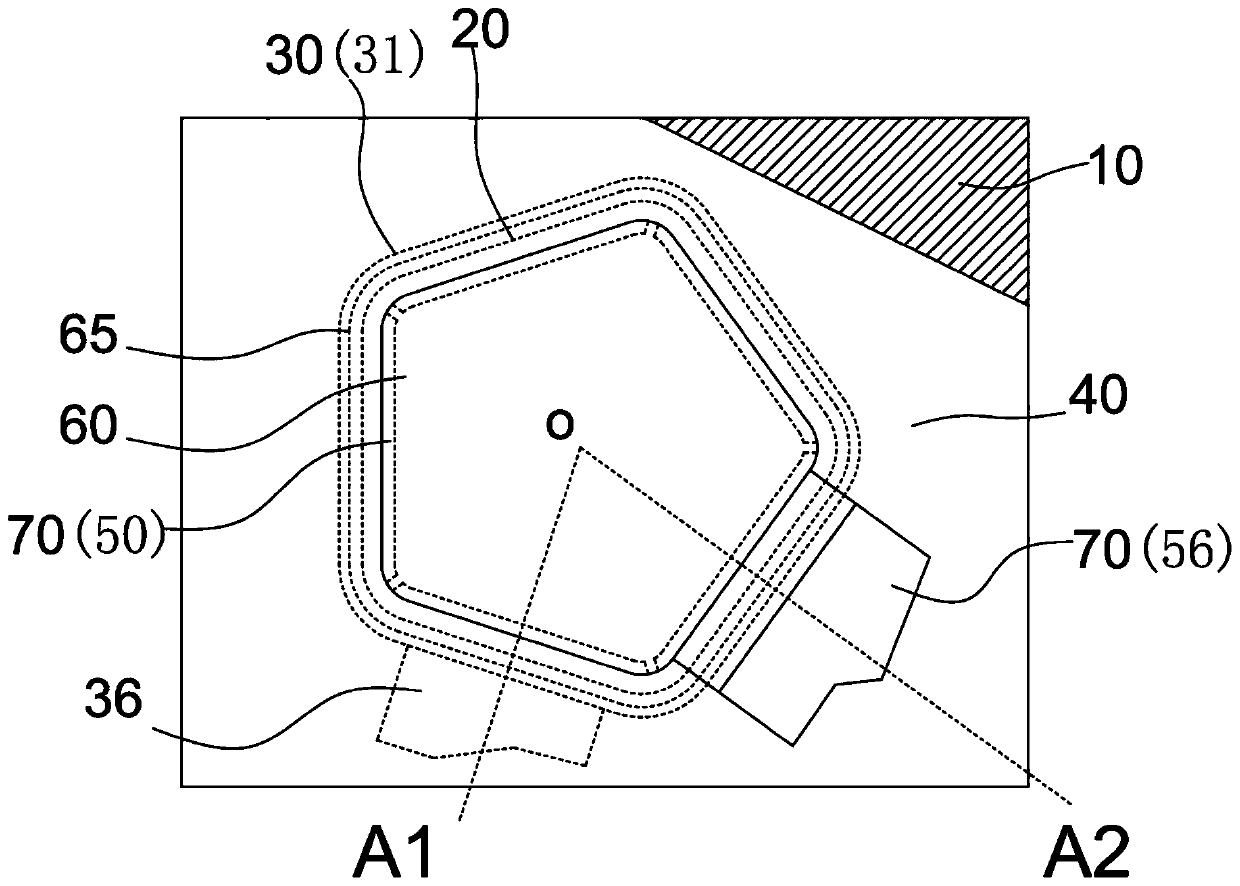
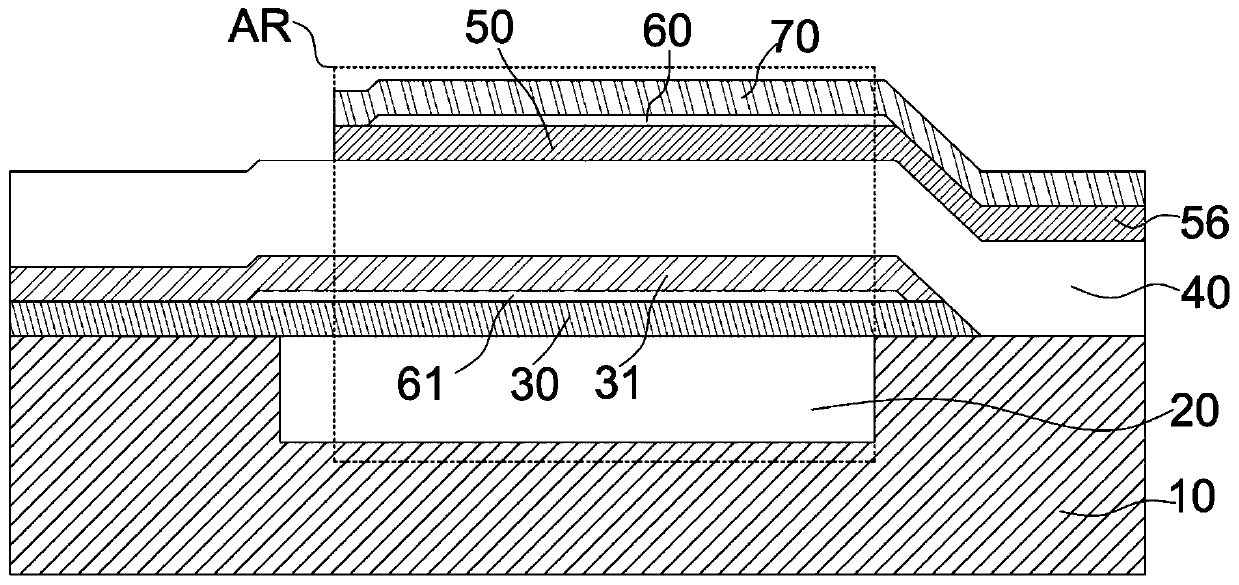
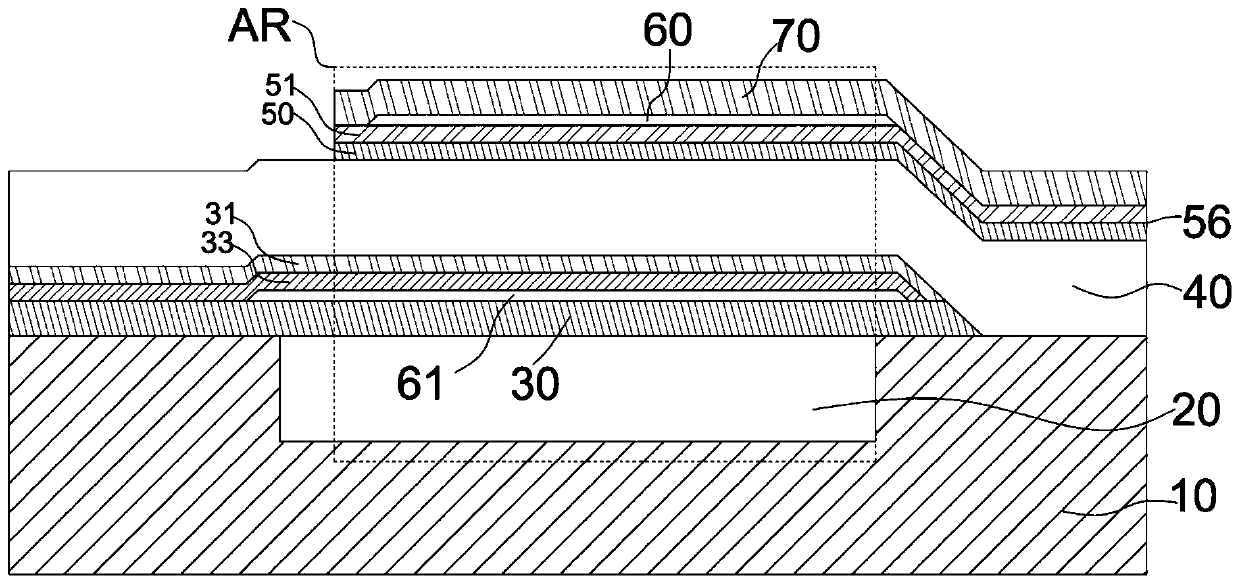
[0025] figure 1 Is a schematic top view of a bulk acoustic wave resonator according to an exemplary embodiment of the present invention, figure 2 Is the edge according to an exemplary embodiment of the present invention figure 1 The schematic cross-sectional view taken from A1-A2 in the figure, where the electrode layer close to the piezoelectric layer has a single-layer structure. in figure 1 with 2 In, the reference signs are as follows:

[0026] 10: S...


PUM


Abstract

The present invention relates to a bulk acoustic wave resonator, and the bulk acoustic wave resonator comprises a substrate; an acoustic mirror; a bottom electrode; a top electrode; and a piezoelectric layer which is arranged between the bottom electrode and the top electrode; the bottom electrode and / or the top electrode are / is a gap electrode; the gap electrode is provided with a gap layer; a first electrode layer is arranged on the side, close to the piezoelectric layer, of the gap layer, a second electrode layer is arranged on the side, away from the piezoelectric layer, of the gap layer,the gap layer is arranged between the first electrode layer and the second electrode layer in the thickness direction of the resonator, and the corresponding first electrode layer and second electrodelayer are electrically connected with each other; the resistivity of the first electrode layer is greater than that of the second electrode layer; and / or the acoustic impedance of the first electrodelayer is greater than that of the second electrode layer. The invention further relates to a filter with the resonator and electronic equipment with the filter or the resonator.

Description

Technical field [0001] The embodiments of the present invention relate to the semiconductor field, and in particular to a bulk acoustic wave resonator, a filter having the resonator, and an electronic device having the resonator or the filter. Background technique [0002] As the basic element of electronic equipment, electronic devices have been widely used, and their applications include mobile phones, automobiles, home appliances, etc. In addition, technologies such as artificial intelligence, Internet of Things, and 5G communications that will change the world in the future still need to rely on electronic devices as their foundation. [0003] Electronic devices can exert different characteristics and advantages according to different working principles. Among all electronic devices, devices that use the piezoelectric effect (or inverse piezoelectric effect) are a very important category. Piezoelectric devices have a very wide range of application scenarios. . Film Bulk Acous...

Claims


Application Information

Patent Timeline
Patent Type & Authority Applications(China)
IPC IPC(8): H03H9/02H03H9/17
CPCH03H9/02007H03H9/02118H03H9/131H03H9/173
Inventor 庞慰张巍郝龙徐洋杨清瑞张孟伦
Owner ROFS MICROSYST TIANJIN CO LTD
Learn More