A kind of silicon dioxide film material with high insulation resistance and preparation method thereof

A technology of silicon dioxide and thin film materials, which is applied to the surface pretreatment, devices for coating liquid on the surface, coatings, etc. The effect of large-scale industrial production, simple preparation method and high insulation resistance

Active Publication Date: 2022-05-13
DALIAN JIAOTONG UNIVERSITY
View PDF2 Cites 0 Cited by
  • Summary
  • Abstract
  • Description
  • Claims
  • Application Information

AI Technical Summary

Problems solved by technology

[0003] At present, silicon dioxide thin films are mostly prepared by thermal oxidation technology. However, thermal oxidation technology needs to heat the substrate to above 1000°C when preparing silicon dioxide thin films, and the substrate can only be single crystal silicon, which limits the thermal oxidation. Preparation of High Insulation Silicon Dioxide Films on Metal Substrates by Oxidation Technology
Chemical vapor deposition technology is also a common method for preparing silicon dioxide films. However, the silicon dioxide films prepared by chemical vapor deposition technology contain a large amount of chemical bonds Si-H, which reduces the insulating properties of silicon dioxide films, and the substrate temperature is also low. Above 200°C, which also limits the preparation of highly insulating silicon dioxide films on metal substrates by chemical vapor deposition
Magnetron sputtering technology is also a common method for preparing silicon dioxide films. However, when preparing silicon dioxide films by magnetron sputtering technology, the substrate is required to be a planar structure, and silicon dioxide films cannot be uniformly prepared on complex curved surfaces. Limiting magnetron sputtering technology to prepare highly insulating silicon dioxide films on the surface of metal substrates with complex curved surface structures
Silicon dioxide thin films can also be prepared by other methods, such as: ion beam sputtering deposition technology, atomic layer deposition technology, chemical water bath synthesis technology, sol-gel technology, etc., but there are some shortcomings in the above technologies, for example: cannot Preparation of highly insulating silicon dioxide film on the surface of a metal substrate with a complex curved surface structure; the prepared silicon dioxide film material has low density, poor insulation, and poor bonding between the film and the substrate; in the process of preparing the silicon dioxide film material, it is necessary to High temperature heat treatment has problems such as long time consumption and low efficiency

Method used


Image

  • A kind of silicon dioxide film material with high insulation resistance and preparation method thereof
  • A kind of silicon dioxide film material with high insulation resistance and preparation method thereof

Examples


Embodiment 1

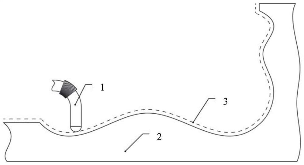
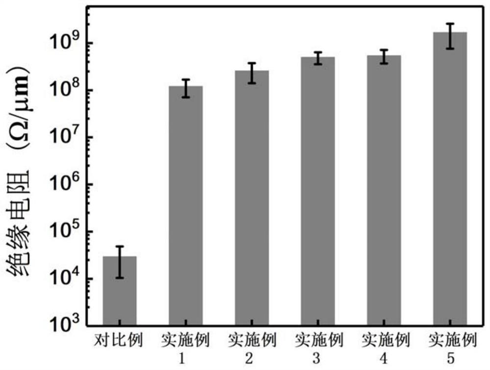
[0033] A method for preparing a silicon dioxide thin film material with high insulation resistance, the preparation method is: using an atmospheric pressure discharge device at room temperature, using a metal substrate with any shape as the base material, using argon with a purity of 99.99% as the discharge gas and carrier Gas, using oxygen with a purity of 99.99% as the reaction gas, and silicon tetrachloride with a purity of 99.99% as the reaction liquid, carry out atmospheric pressure discharge to prepare a silicon dioxide film, and maintain a constant distance between the nozzle of the atmospheric pressure discharge device and the surface of the substrate, and obtain The thickness of silicon dioxide film is 1.31μm, and its insulation resistance is 1.55±0.53×10 8 Ω, calculated according to the linear relationship between the insulation resistance of the silicon dioxide film material and its thickness, the insulation resistance of the silicon dioxide film material is 1.19 ± 0...

Embodiment 2

[0036] A method for preparing a silicon dioxide thin film material with high insulation resistance, the preparation method is: using an atmospheric pressure discharge device at room temperature, using a metal substrate with any shape as the base material, using argon with a purity of 99.99% as the discharge gas and carrier Gas, using oxygen with a purity of 99.99% as the reaction gas, and silicon tetrachloride with a purity of 99.99% as the reaction liquid, carry out atmospheric pressure discharge to prepare a silicon dioxide film, and maintain a constant distance between the nozzle of the atmospheric pressure discharge device and the surface of the substrate, and obtain The thickness of silicon dioxide film is 4.86μm, and its insulation resistance is 1.25±0.14×10 9 Ω, calculated according to the linear relationship between the insulation resistance of the silicon dioxide film material and its thickness, the insulation resistance of the silicon dioxide film material is 2.57 ± 0...

Embodiment 3

[0039] A method for preparing a silicon dioxide thin film material with high insulation resistance, the preparation method is: using an atmospheric pressure discharge device at room temperature, using a metal substrate with any shape as the base material, using argon with a purity of 99.99% as the discharge gas and carrier Gas, using oxygen with a purity of 99.99% as the reaction gas, and silicon tetrachloride with a purity of 99.99% as the reaction liquid, carry out atmospheric pressure discharge to prepare a silicon dioxide film, and maintain a constant distance between the nozzle of the atmospheric pressure discharge device and the surface of the substrate, and obtain The thickness of silicon dioxide film is 5.38μm, and its insulation resistance is 2.67±0.32×10 9 Ω, calculated according to the linear relationship between the insulation resistance of the silicon dioxide film material and its thickness, the insulation resistance of the silicon dioxide film material is 4.96 ± 0...


PUM

PropertyMeasurementUnit
thicknessaaaaaaaaaa
thicknessaaaaaaaaaa
thicknessaaaaaaaaaa

Abstract

The invention relates to a silicon dioxide thin film material with high insulation resistance and a preparation method thereof, belonging to the technical fields of surface processing, coating and thin film materials. The preparation method of the present invention is: using the method of atmospheric pressure discharge to obtain silicon dioxide film material with high insulation resistance, the temperature of atmospheric pressure discharge is room temperature, and during the growth process of silicon dioxide film, the nozzle of the atmospheric pressure discharge device is always perpendicular to the substrate surface, the nozzle keeps a constant distance from the surface of the substrate, and the nozzle makes periodic reciprocating movements relative to the surface of the substrate. Compared with the existing silicon dioxide thin film material, the high insulation resistance silicon dioxide film material of the present invention has high insulation resistance.

Description

technical field [0001] The invention relates to a silicon dioxide thin film material with high insulation resistance and a preparation method thereof, belonging to the technical fields of surface processing, coating and thin film materials. Background technique [0002] Silicon Dioxide (Silicon Dioxide, SiO 2 ) Thin film materials are an important class of high insulation resistance materials, which have important applications in the fields of thin film sensors and integrated circuits, such as: the insulating layer between the metal substrate and the thin film thermocouple temperature sensor, insulation layer etc. [0003] At present, silicon dioxide thin films are mostly prepared by thermal oxidation technology. However, thermal oxidation technology needs to heat the substrate to above 1000°C when preparing silicon dioxide thin films, and the substrate can only be single crystal silicon, which limits the thermal oxidation. Oxidation technology prepares highly insulating s...

Claims


Application Information

Patent Timeline
Patent Type & Authority Patents(China)
IPC IPC(8): B05D1/04B05D3/04
CPCB05D1/04B05D3/0486
Inventor 丁万昱王棋震
Owner DALIAN JIAOTONG UNIVERSITY
Why Eureka
Try Eureka