Chip interconnection structure, chip and chip interconnection method

An interconnection structure and chip technology, applied in the direction of semiconductor/solid-state device components, semiconductor devices, electrical components, etc., can solve the problems of excessively long leads and substrate windings, increasing power, and increasing production costs.

Pending Publication Date: 2020-05-01
SHENZHEN GOODIX TECH CO LTD
View PDF0 Cites 0 Cited by
  • Summary
  • Abstract
  • Description
  • Claims
  • Application Information

AI Technical Summary

Problems solved by technology

[0004] However, when using the above-mentioned traditional packaging method to realize the interconnection between two or more chips, because the lead wires and substrate winding wires used for the interconnection of two or more chips are too long, the resistance will increase, which will lead to a decrease in communi

Method used


Image

  • Chip interconnection structure, chip and chip interconnection method
  • Chip interconnection structure, chip and chip interconnection method
  • Chip interconnection structure, chip and chip interconnection method

Examples


Embodiment 1

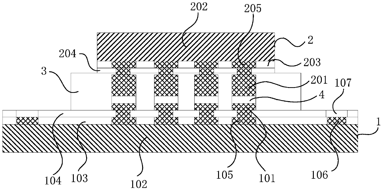
[0073] figure 1 is a schematic structural diagram of the chip interconnection structure provided in Embodiment 1 of the present application, figure 2 It is a schematic structural diagram of another chip interconnection structure provided in Embodiment 1 of the present application.

[0074] The chip interconnection structure provided by this embodiment can be used for the interconnection between chips in the field of semiconductor technicians, and is especially suitable for the interconnection between chips that require interconnection communication. The chip interconnection structure provided by this embodiment realizes two One or more chips are interconnected and the purpose of high-speed communication of the interconnected chips can be realized, which solves the technical problem in the prior art that the communication speed decreases when the chips are interconnected.

[0075] like figure 1 and figure 2 As shown, the chip interconnection structure includes: a first chi...

Embodiment 2

[0094] Further, on the basis of the foregoing embodiments, in this embodiment, as figure 1 and image 3 As shown, each conductive component includes at least two conductive elements connected in sequence, and the pads of the first chip 1 and the pads of the second chip 2 are connected through two or two conductive elements connected in sequence.

[0095] Among them, in this embodiment, such as figure 1 and image 3 As shown, each conductive component includes a first conductive member 101 and a second conductive member 201, the first end of the first conductive member 101 is connected to the pad of the first chip 1, and the second end of the first conductive member 101 is connected to the first conductive member 101. The first ends of the two conductive elements 201 are connected to each other, and the second ends of the second conductive elements 201 are connected to the pads of the second chip 2 .

[0096] It should be noted that the first conductive member 101 is connect...

Embodiment 3

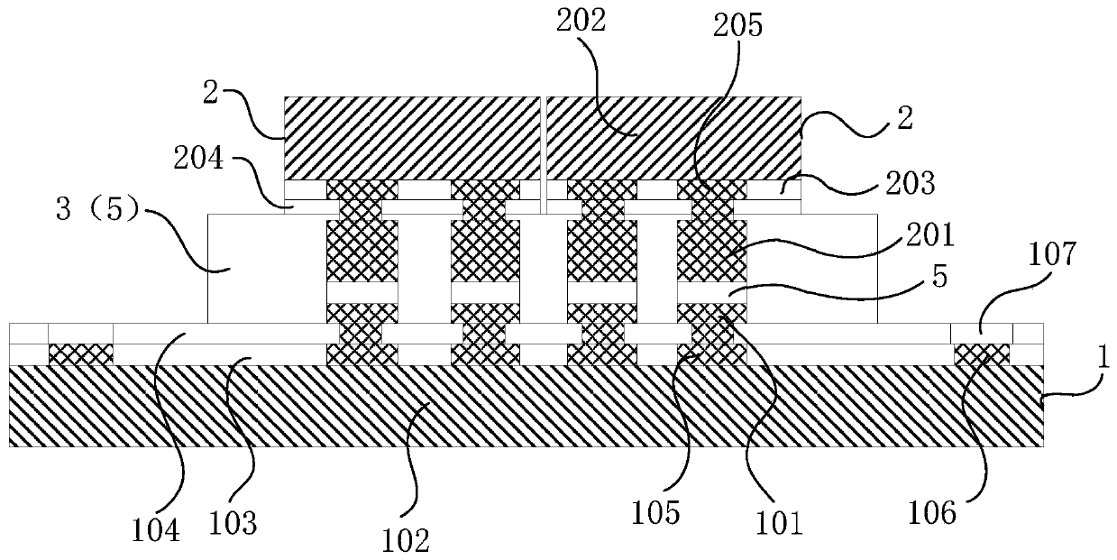
[0110] Further, on the basis of the foregoing embodiments, in this embodiment, as figure 2 As shown, the number of second chips 2 is at least two, and the second chips 2 are all arranged on the same side of the first chip 1 , or the second chips 2 are arranged on the front and back sides of the first chip 1 .

[0111] It should be noted that, in this embodiment, if figure 2 As shown, when the number of second chips 2 is two or more, the second chips 2 can be arranged on the same side of the first chip 1, and the transfer surfaces of all the second chips 2 are connected to the first chip 1. The transfer surfaces are oppositely arranged, and are connected between the pads of the first chip 1 and the pads of the second chip 2 through conductive members; the second chip 2 can be arranged on both sides of the first chip 1, that is, the second The chips 2 can be evenly distributed on the front and back sides of the first chip 1. At this time, the front and back sides of the first...


PUM


Abstract

The application provides a chip interconnection structure, a chip and a chip interconnection method. The chip interconnection structure includes a first chip and at least one second chip, wherein theswitching face of the first chip is opposite to the switching face of the second chip, at least one conducting component is arranged between the second chip and the first chip, every conducting component includes at least one electrically conductive piece connected between the bonding pad of the second chip and the bonding pad of the first chip. The chip interconnection structure can make two or more chips interconnected and communicate with each other at a high speed.

Description

technical field [0001] The present application relates to the technical field of semiconductor manufacturing, and in particular to a chip interconnection structure, a chip and a chip interconnection method. Background technique [0002] With the development of semiconductor technology, the chip size tends to be miniaturized, and the development of technology requires higher and higher communication speed of the chip. [0003] At present, the traditional packaging method relies on wire bonding and circuit board substrate to connect two or more chips, so as to realize the interconnection of pins between chips and complete communication. Among them, wire bonding is called pressure welding, which refers to the use of metal wires to use thermal pressure or ultrasonic energy to complete the connection of internal interconnection wires in solid-state circuits in microelectronic devices, that is, the connection between chips and circuits or lead frames, which is common in surface pa...

Claims


Application Information

Patent Timeline
IPC IPC(8): H01L25/18H01L23/52H01L21/768H01L21/98
CPCH01L25/18H01L23/52H01L21/768H01L25/50H01L24/13H01L24/16H01L2224/73204H01L2224/16145H01L2224/32145H01L24/32H01L24/29H01L25/0657H01L2224/32013H01L2224/32014H01L2225/06513H01L2225/06568H01L2224/13111H01L2224/13144H01L2224/13147H01L2224/13124H01L2224/81815H01L2224/81805H01L2224/812H01L2224/81205H01L2224/83101H01L2224/83851H01L2224/1329H01L2224/13339H01L2224/92125H01L2224/73207H01L2224/2919H01L2224/05611H01L2224/05624H01L2224/05644H01L2224/05647H01L2224/13014H01L2224/13012H01L2224/05555H01L2224/05552H01L2224/1145H01L2224/11464H01L2224/11462H01L2224/1132H01L2224/0332H01L2224/0345H01L2224/03462H01L2224/03464H01L2224/03332H01L2224/11332H01L2224/05166H01L2224/0347H01L2224/1147H01L2224/0361H01L2224/03912H01L2224/03914H01L2224/0391H01L24/94H01L24/81H01L24/83H01L2224/81903H01L2224/9211H01L24/92H01L21/563H01L2224/83104H01L2224/83102H01L24/03H01L24/05H01L2224/0401H01L2224/04042H01L24/11H01L2224/94H01L2224/92H01L24/73H01L2224/13006H01L2224/16502H01L2924/00014H01L2924/00012H01L2924/0665H01L2224/81H01L2224/83H01L2224/03H01L2224/11H01L21/78H01L2924/00H01L2224/13139H01L2224/81238H01L2225/06558
Inventor 冷寒剑吴宝全
Owner SHENZHEN GOODIX TECH CO LTD
Why Eureka
Try Eureka