

Filling method of redundant metal
A filling method and technology of redundant graphics, applied in special data processing applications, instruments, electrical digital data processing, etc., can solve problems such as large differences in the density of redundant graphics
- Summary
- Abstract
- Description
- Claims
- Application Information
AI Technical Summary
Problems solved by technology
Method used
Image

Examples
Embodiment 1
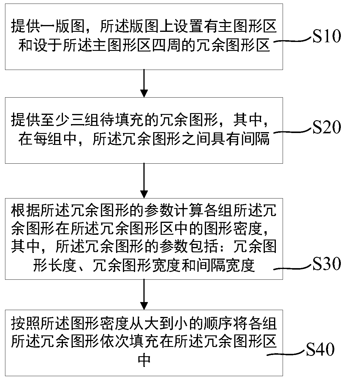
[0041] The present invention provides a filling method of redundant graphics, refer to figure 1 , figure 1 It is a flowchart of a method for filling redundant graphics in Embodiment 1 of the present invention. In this embodiment, the method for filling redundant graphics includes:
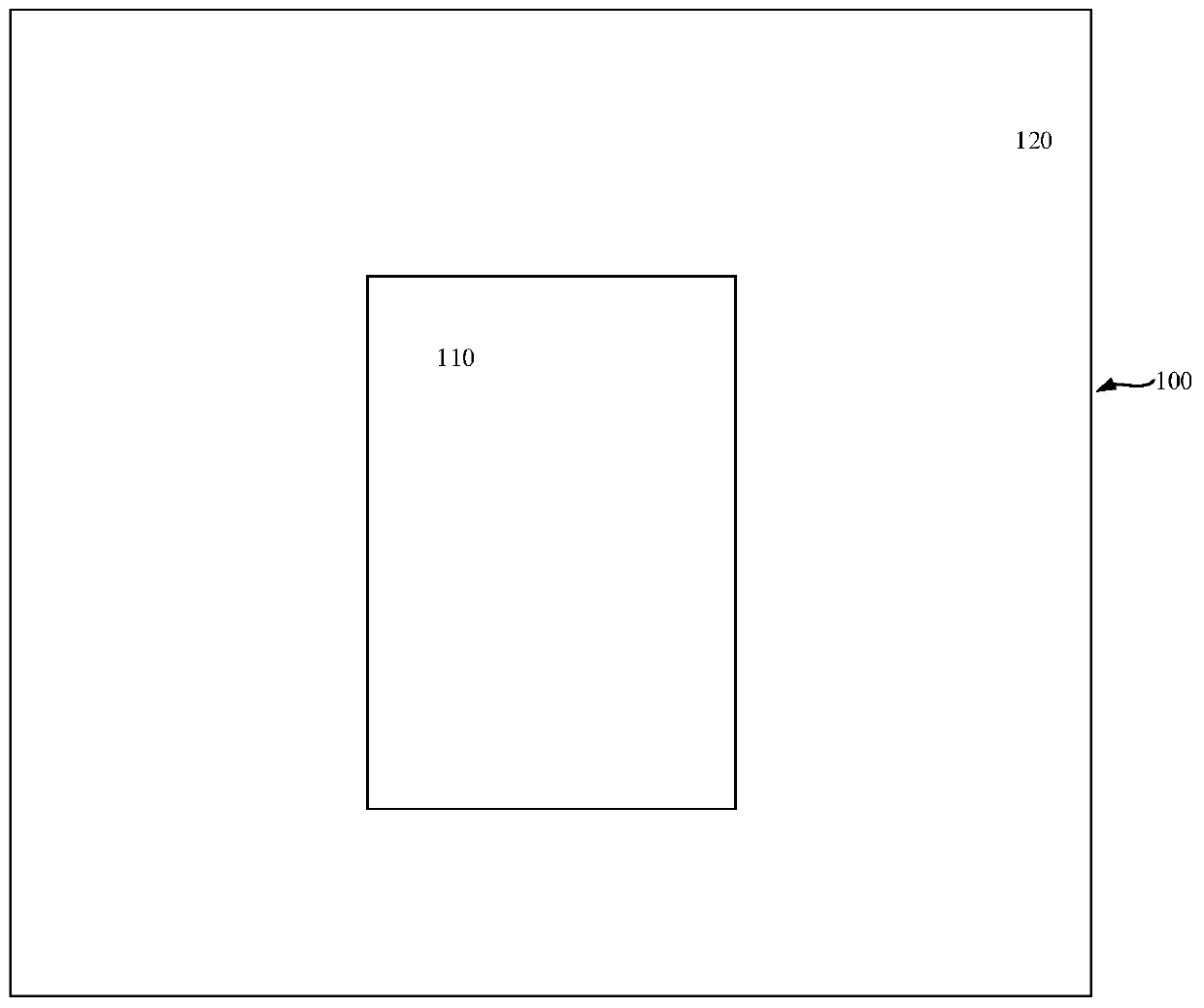
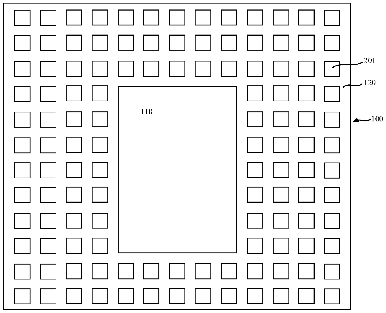
[0042] S10: providing a layout, the layout is provided with a main graphics area and redundant graphics areas around the main graphics area;
[0043] S20: providing at least three groups of redundant graphics to be filled, wherein, in each group, there is an interval between the redundant graphics;
[0044] S30: Calculate the pattern density of each group of redundant patterns in the redundant pattern area according to the parameters of the redundant patterns, wherein the parameters of the redundant patterns include: redundant pattern length, redundant pattern width and interval width;
[0045] S40: Fill each group of redundant graphics in the redundant graphics area sequentially in descending o...
Embodiment 2
[0055] In this example, refer to Figure 6 , Figure 6 It is a flowchart of a method for filling redundant graphics according to Embodiment 2 of the present invention, and the method for filling redundant graphics includes:
[0056] S10: providing a layout, the layout is provided with a main graphics area and redundant graphics areas around the main graphics area;
[0057] S20: providing at least three groups of redundant graphics to be filled, wherein, in each group, there is an interval between the redundant graphics;
[0058] S30: Calculate the pattern density of each group of redundant patterns in the redundant pattern area according to the parameters of the redundant patterns, wherein the parameters of the redundant patterns include: redundant pattern length, redundant pattern width and interval width;
[0059] S40: Divide the redundant graphic area into a first graphic area, a second graphic area to an n-th graphic area in the order from the redundant graphic area to ...
PUM
| Property | Measurement | Unit |
|---|---|---|
| Length | aaaaa | aaaaa |
| Interval width | aaaaa | aaaaa |
| Length | aaaaa | aaaaa |
Abstract
Description
Claims
Application Information