Method for forming semiconductor memory

A memory and semiconductor technology, applied in the fields of semiconductor devices, semiconductor/solid-state device manufacturing, electric solid-state devices, etc., can solve the problems of high manufacturing cost and complicated semiconductor memory manufacturing process, and achieve simplified manufacturing process, uniform pattern layout density, The effect of increasing graphics density

Active Publication Date: 2022-03-18
CHANGXIN MEMORY TECH INC
View PDF18 Cites 0 Cited by
  • Summary
  • Abstract
  • Description
  • Claims
  • Application Information

AI Technical Summary

Problems solved by technology

[0003] In the existing method for forming a semiconductor memory, when preparing the bit line and the peripheral gate layer of the peripheral transistor, it is usually necessary to form them separately in different process steps, which will inevitably lead to a relatively complicated manufacturing process of the semiconductor memory, and the preparation The cost is also higher

Method used


Image

  • Method for forming semiconductor memory
  • Method for forming semiconductor memory
  • Method for forming semiconductor memory

Examples


Embodiment Construction

[0057] The method for forming the semiconductor memory proposed by the present invention will be further described in detail below with reference to the accompanying drawings and specific embodiments. The advantages and features of the present invention will become clearer from the following description. It should be noted that all the drawings are in a very simplified form and use imprecise scales, and are only used to facilitate and clearly assist the purpose of illustrating the embodiments of the present invention.

[0058] Preferred embodiments of the invention are shown in the following examples, it being understood that those skilled in the art may modify the invention described herein and still achieve the beneficial effects of the invention. Therefore, the following description should be understood as the broad knowledge of those skilled in the art, but not as a limitation of the present invention.

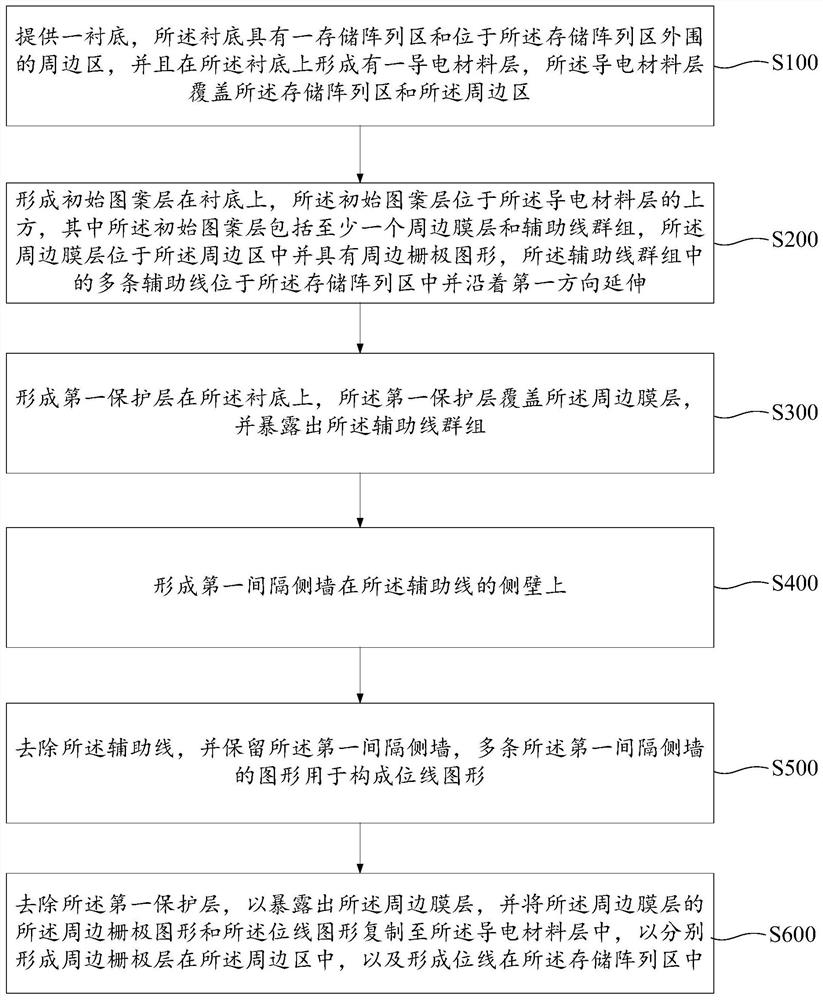
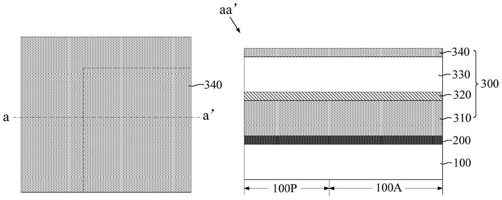
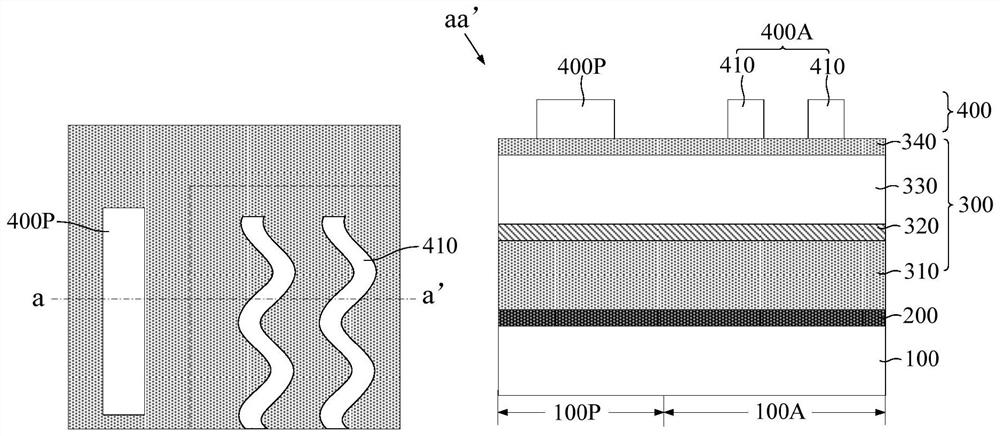
[0059] figure 1 It is a schematic flow chart of a method for formin...


PUM

PropertyMeasurementUnit
hardnessaaaaaaaaaa

Abstract

The invention provides a method for forming a semiconductor memory. At the same time, the auxiliary line group and the peripheral film layer located on the periphery of the auxiliary line group are prepared, and the bit line pattern is further defined based on the auxiliary line group in the auxiliary line group, so that the peripheral gate pattern of the peripheral film layer and the bit line The line pattern is simultaneously copied into the conductive material layer to simultaneously form the peripheral gate layer and the bit line. In this way, the manufacturing process of the semiconductor memory can be effectively simplified, and the cost can be saved, and at the same time, the abnormal shape of the bit line at the edge position can be improved.

Description

technical field [0001] The invention relates to the technical field of semiconductors, in particular to a method for forming a semiconductor memory. Background technique [0002] A semiconductor memory (eg, dynamic random access memory, DRAM) generally includes a memory cell array for storing data, and peripheral circuits located around the memory cell array. Wherein, the memory cell array is composed of a plurality of memory cells arranged in an array in the memory array area, and the memory cells are also connected to a bit line; and, the peripheral circuit usually includes peripheral transistors. [0003] In the existing method for forming a semiconductor memory, when preparing the bit line and the peripheral gate layer of the peripheral transistor, it is usually necessary to form them separately in different process steps, which will inevitably lead to a relatively complicated manufacturing process of the semiconductor memory, and the preparation The cost is also higher...

Claims


Application Information

Patent Timeline
Patent Type & Authority Patents(China)
IPC IPC(8): H01L21/8242H01L27/108
CPCH10B12/482H10B12/09
Inventor 宫光彩
Owner CHANGXIN MEMORY TECH INC
Why Eureka
Try Eureka