Semiconductor structure and forming method thereof

A semiconductor and pattern area technology, applied in semiconductor/solid-state device manufacturing, electrical components, circuits, etc., can solve problems such as device performance and performance uniformity to be improved, avoid etching load effects, increase pattern density, and uniformity. good effect

Pending Publication Date: 2020-08-04
SEMICON MFG INT (SHANGHAI) CORP +1
View PDF3 Cites 0 Cited by
  • Summary
  • Abstract
  • Description
  • Claims
  • Application Information

AI Technical Summary

Problems solved by technology

[0003] However, the performance and performance uniformity of devices formed by existing processes need to be improved

Method used


Image

  • Semiconductor structure and forming method thereof
  • Semiconductor structure and forming method thereof
  • Semiconductor structure and forming method thereof

Examples


Embodiment Construction

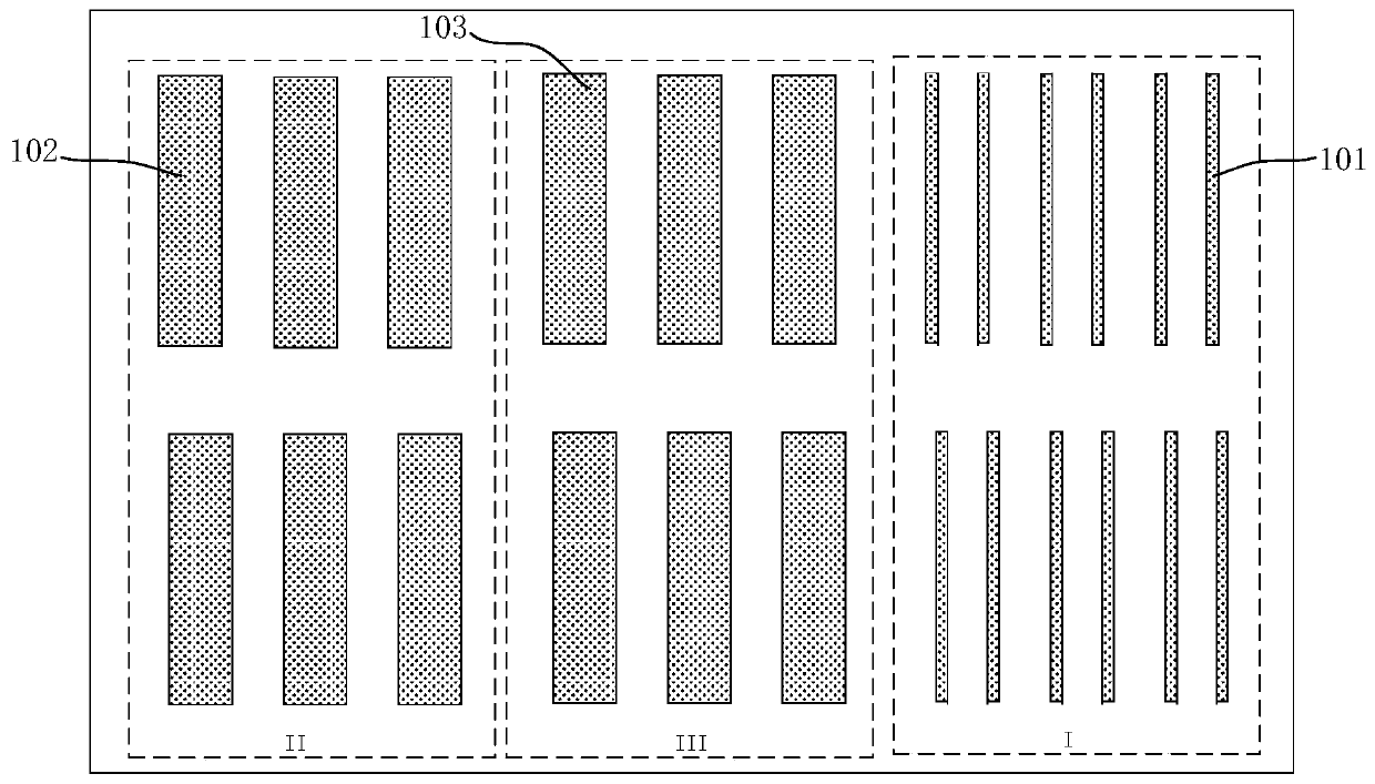
[0012] It can be seen from the background art that the performance and performance uniformity of devices formed by existing processes still need to be improved. The reason why the performance of the device needs to be improved is analyzed in combination with a method of forming a semiconductor structure.

[0013] Specifically, in the process of forming the gate structure, mask patterns of different sizes are formed through different processes, for example, refer to figure 1 A mask pattern layout structure diagram shown in , a small-size mask pattern 101 is formed in the GM region I by a self-aligned double patterning (self-aligned double patterning, SADP) process, and a photolithography and etching process A large-size mask pattern 102 is formed in the GT region II, and then a gate structure of a corresponding size is formed by etching using the two mask patterns as a mask. However, in the process of forming mask patterns of different sizes, due to the low pattern density, th...


PUM

PropertyMeasurementUnit
thicknessaaaaaaaaaa
heightaaaaaaaaaa
thicknessaaaaaaaaaa

Abstract

The invention discloses a semiconductor structure and a forming method thereof, and the method comprises the steps: providing a substrate which comprises a first pattern region, a second pattern region and an auxiliary region, the size of a target pattern formed in the first pattern region being smaller than the size of a target pattern formed in the second pattern region; forming a first mask pattern on the substrate in the first pattern region and the auxiliary region; after the first mask pattern is formed, forming a second mask pattern on the substrate in the second pattern region and theauxiliary region, wherein in the auxiliary region, the second mask pattern covers the first mask pattern; and etching the substrate by taking the first mask pattern and the second mask pattern as masks to form the target pattern. In the embodiment of the invention, the uniformity of the target patterns formed in the first pattern region and the second pattern region is improved, and the device performance and the performance uniformity are correspondingly improved.

Description

technical field [0001] The invention relates to the field of semiconductor manufacturing, in particular to a semiconductor structure and a forming method thereof. Background technique [0002] During the formation of semiconductor devices, gate structures of different sizes need to be formed on the substrate. In the layout of the gate structure in the prior art, it is divided into large-scale patterns and small-scale patterns according to the size of the gate structure. Large-scale patterns are usually formed by combining photolithography and etching processes, and small-scale patterns are usually formed by self-alignment double patterning. (self-aligneddouble patterning, SADP) process. [0003] However, the performance and performance uniformity of devices formed by existing processes need to be improved. Contents of the invention [0004] Embodiments of the present invention provide a semiconductor structure and a method for forming the same, so as to improve device pe...

Claims


Application Information

Patent Timeline
Patent Type & Authority Applications(China)
IPC IPC(8): H01L21/033
CPCH01L21/033H01L21/0334
Inventor 舒强张迎春覃柳莎
Owner SEMICON MFG INT (SHANGHAI) CORP
Why Eureka
Try Eureka