
Triple Graphical Approach

A re-patterning and patterning technology, applied in the manufacturing of electrical components, circuits, semiconductor/solid-state devices, etc., can solve problems such as increasing pattern density, pattern size process limitations, and complex manufacturing processes

Active Publication Date: 2020-02-07
SEMICON MFG INT (SHANGHAI) CORP +1
View PDF7 Cites 0 Cited by
  • Summary
  • Abstract
  • Description
  • Claims
  • Application Information

AI Technical Summary

Problems solved by technology

Among them, the LELE method can be divided into two types according to the pattern type: etching trench (trench) / via (via) shape and line (line) / space (space) shape, and for the latter etching line / space shape Dual patterning manufacturing process is often too complex
[0004] The SADP method is widely used because of its simple process, and it can also increase the pattern density on the semiconductor substrate and reduce the distance between adjacent patterns to a certain extent, but the pattern size formed by the self-aligned double patterning method is still Limited by the process, the demand for more complex technology still faces the problem of increasing the pattern density

Method used


Image

  • Triple Graphical Approach
  • Triple Graphical Approach
  • Triple Graphical Approach

Examples


Embodiment Construction

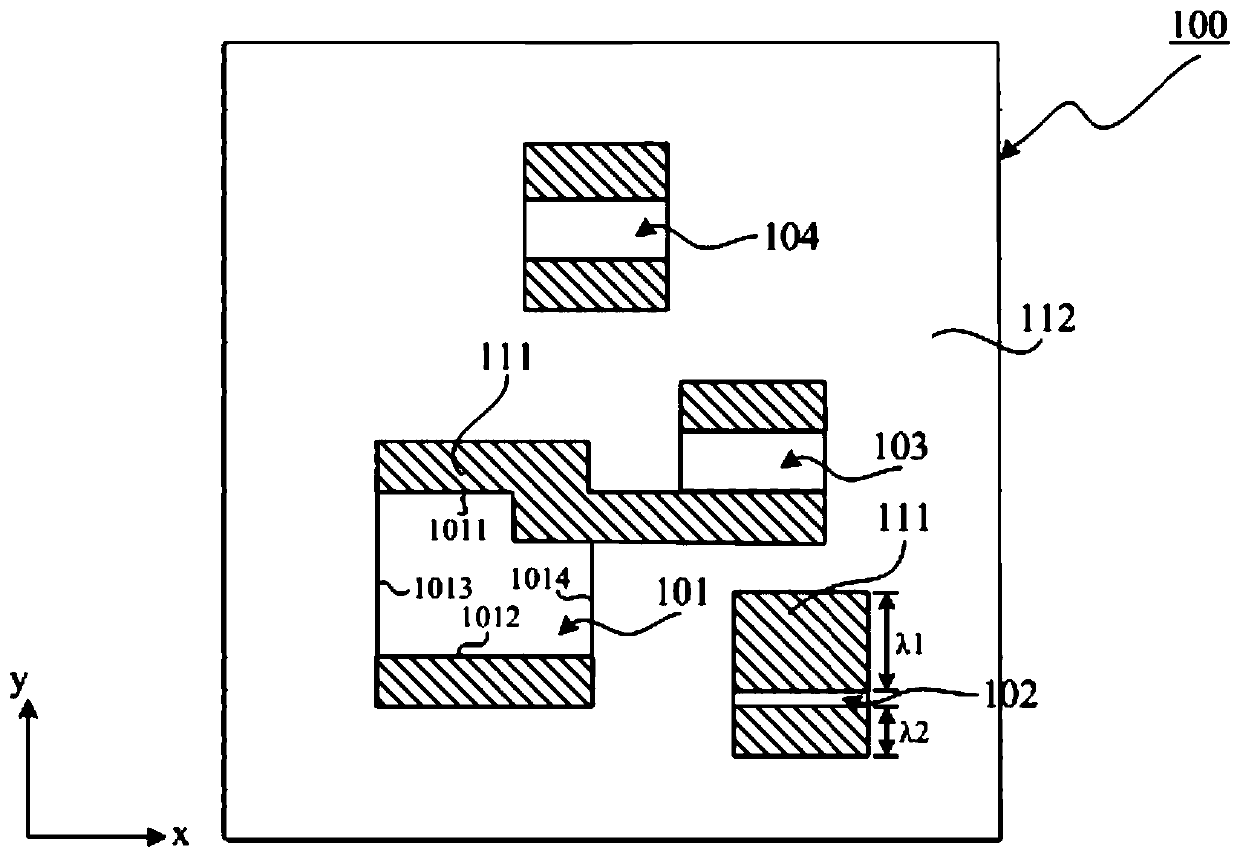
[0033] refer to figure 1 , is a schematic diagram of the structure of an intermediate step in a dual patterning method.

[0034] A substrate is provided, and a mask layer 100 is formed on the surface of the substrate.

[0035] Target graphics are provided, including target graphics 101 , 102 , 103 and 104 , and the target graphics are used to define areas to be patterned on the substrate. Here, the method of double graphics is described by taking the target graphics 101 as an example. First use the first reticle to pattern the mask layer 100, remove the first part of the mask layer 111, to define the first boundary 1011 and the second boundary 1012 of the target pattern 101 along the x direction, and then use The second mask plate performs patterning on the mask layer 100 to remove the second part of the mask layer 112 to define the third boundary 1013 and the fourth boundary 1014 of the target pattern 101 along the y direction.

[0036] The size of the pattern formed by th...


PUM


Abstract

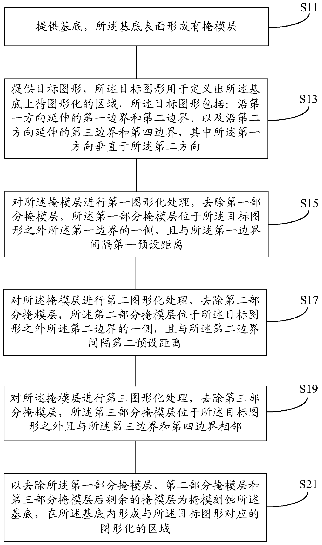
Disclosed is a triple patterning method, comprising the steps of: providing a substrate, a mask layer being formed on the surface of the substrate; providing a target pattern, and defining an area tobe patterned on the substrate, the target pattern comprising a first boundary and a second boundary extending along a first direction as well as a third boundary and a fourth boundary extending alonga second direction; performing first patterning on the mask layer to remove a first portion of the mask layer, the first portion of the mask layer being spaced from the first boundary a first predetermined distance; performing second patterning on the mask layer to remove a second portion of the mask layer, the second portion of the mask layer being spaced from the second boundary a second predetermined distance; performing third patterning on the mask layer to remove a third portion of the mask layer, the third portion of the mask layer being outside the target pattern and adjacent to the third boundary and the fourth boundary; and etching the substrate using the remaining mask layer as a mask to form a patterned area. The triple patterning method increases the pattern density on the substrate and reduces the pattern distance.

Description

technical field [0001] The invention relates to a patterning method in the field of semiconductor manufacturing, in particular to a triple patterning method. Background technique [0002] In the semiconductor manufacturing process, photolithography is a commonly used patterning method. However, the photolithography process will limit the minimum pitch of the formed pattern, and thus also limit the development of integrated circuits in the direction of smaller size and higher density. [0003] Double patterning technology (Double Patterning Technology, DPT) is a kind of method that can make the lithography process overcome the lithography resolution limit. Double patterning mainly includes two traditional methods: Litho-Etch-Litho-Etch (LELE) and Self-aligned Double Patterning (SADP). Among them, the LELE method can be divided into two types according to the pattern type: etching trench (trench) / via (via) shape and line (line) / space (space) shape, and for the latter etching...

Claims


Application Information

Patent Timeline
Patent Type & Authority Patents(China)
IPC IPC(8): H01L21/033
CPCH01L21/0337H01L21/0338
Inventor 沈忆华余云初
Owner SEMICON MFG INT (SHANGHAI) CORP
Learn More