Target system and method of determining alignment error in electronic substrates

A technique for measuring tools and alignment errors, applied in the photoengraving process, circuits, electrical components, etc. of the pattern surface

Inactive Publication Date: 2007-08-15
INT BUSINESS MASCH CORP
View PDF7 Cites 0 Cited by
  • Summary
  • Abstract
  • Description
  • Claims
  • Application Information

AI Technical Summary

Problems solved by technology

[0007] Although overlapping targets disclosed in the prior art individually satisfy some of the above criteria, there is still a need for overlapping targets optimized under all constraints

Method used


Image

  • Target system and method of determining alignment error in electronic substrates
  • Target system and method of determining alignment error in electronic substrates
  • Target system and method of determining alignment error in electronic substrates

Examples


Embodiment Construction

[0039] In describing the preferred embodiment of the invention, reference will be made to the accompanying drawings 2-14, wherein like numerals indicate like parts of the invention.

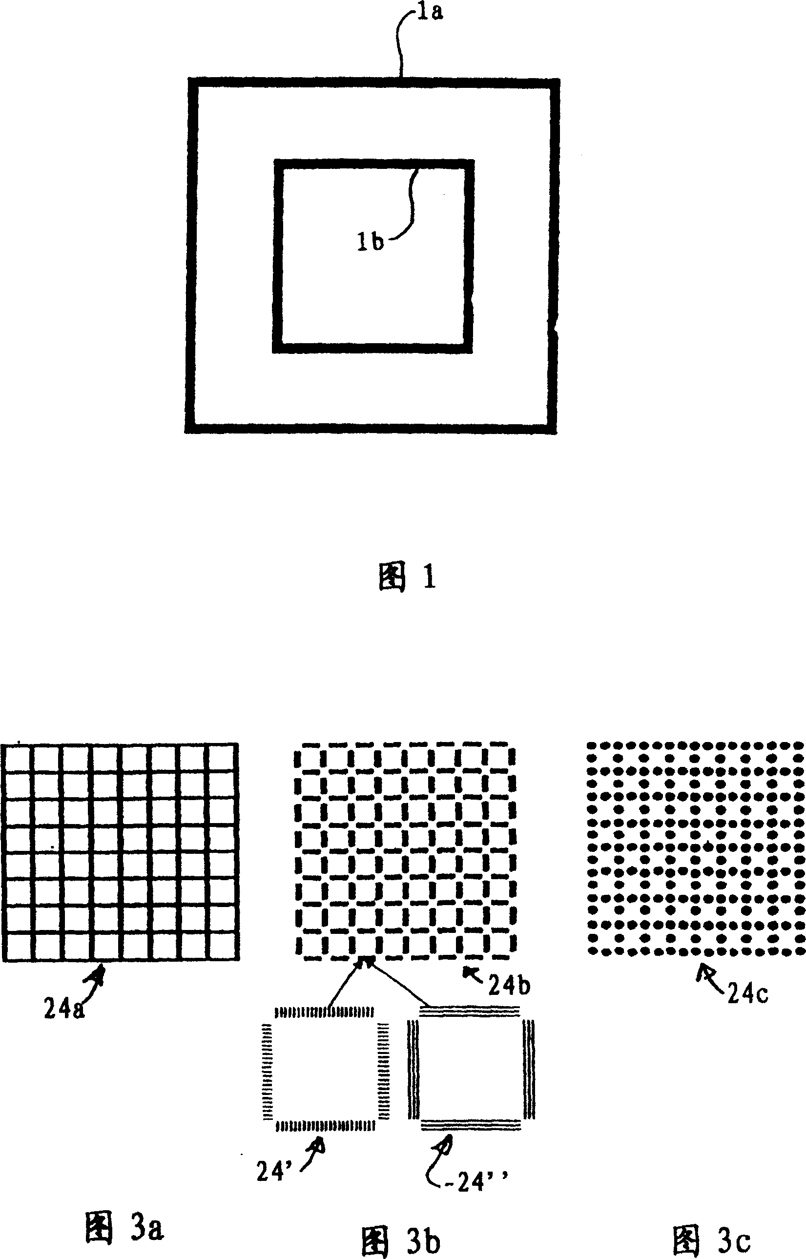
[0040] Figure 2 shows an example of overlapping targets of the present invention. The overlay target 20 is composed of nested grid patterns, with the outer pattern 22 serving as a reference grid and the plurality of sub-patterns 24 serving as sub-grids. The area of ​​reference grid portions of overlapping targets is divided into an N x M array of preferably equal area grid portions, called boxes, represented by a reference grid pattern of period D printed on the first layer of the patterning sequence. The reference grid includes at least one row of connected boxes, ie a plurality of grid segments in at least one direction of x and y, such that N is greater than or equal to one and M is greater than one. Preferably, the array has a plurality of grid segments in both the x and y directions such th...


PUM

PropertyMeasurementUnit
wavelengthaaaaaaaaaa

Abstract

A method of determining alignment error in electronic substrates comprises providing on a layer of a substrate a first contrasting set of elements forming a first grid pattern having a plurality of grid segments in the x and y directions. The method also includes providing nested within at least one of the first grid pattern segments, on the same or different layer of a substrate, a second contrasting set of elements forming a second grid pattern having a plurality of grid segments in the x and y directions. The method then includes determining the center of the first set of elements in the first grid pattern and determining the center of the second set of elements in the second grid pattern. The method then comprises comparing the centers of the first and second sets of elements and determining alignment error of the first and second grid patterns.

Description

technical field [0001] The present invention relates generally to semiconductor manufacturing, and more particularly to overlay measurement targets and methods for controlling alignment errors in different patterned layers of a semiconductor wafer stack and in different patterns on the same layer. Background technique [0002] Novel measurement methods and lithographic control methods for the overlap control of integrated circuit regions within and between layers of circuits made by lithographic processes are disclosed in US Patent No. 5,877,861. As described in this patent, by photolithographic methods, an exposure tool known as a stepper prints a plurality of integrated circuit patterns or regions (also called product units) on successive layers of a semiconductor wafer. These steppers typically pattern the different layers by employing step-and-repeat lithography exposure or step-and-scan lithography exposure, where the entire wafer is patterned by sequential exposure of ...

Claims


Application Information

Patent Timeline
Patent Type & Authority Patents(China)
IPC IPC(8): H01L21/00G03F7/20
CPCG03F7/70633
Inventor C·P·奥施尼特J·D·莫里洛
Owner INT BUSINESS MASCH CORP
Why Eureka
Try Eureka