Wafer testing method

A test method and wafer technology, applied in the direction of semiconductor/solid-state device test/measurement, electrical components, circuits, etc., can solve the problems of increasing individualized tests, which cannot be realized, and achieve the effect of increasing test items and thorough testing

Pending Publication Date: 2020-05-08
SHANGHAI HUAHONG GRACE SEMICON MFG CORP
View PDF10 Cites 3 Cited by
  • Summary
  • Abstract
  • Description
  • Claims
  • Application Information

AI Technical Summary

Problems solved by technology

[0009] 2. The number of test items is fixed, and the number of test items for each Die ≤ the total test items, so it is impossible to increase the personalized test

Method used


Image

  • Wafer testing method
  • Wafer testing method
  • Wafer testing method

Examples


Embodiment Construction

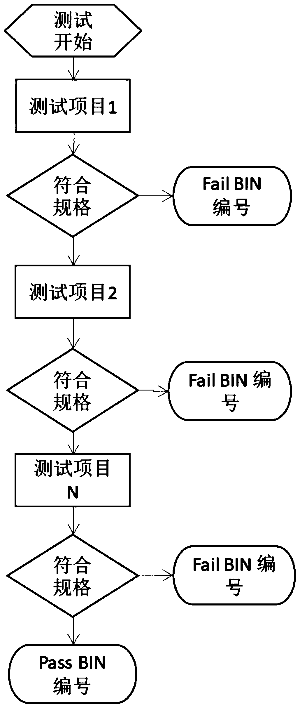
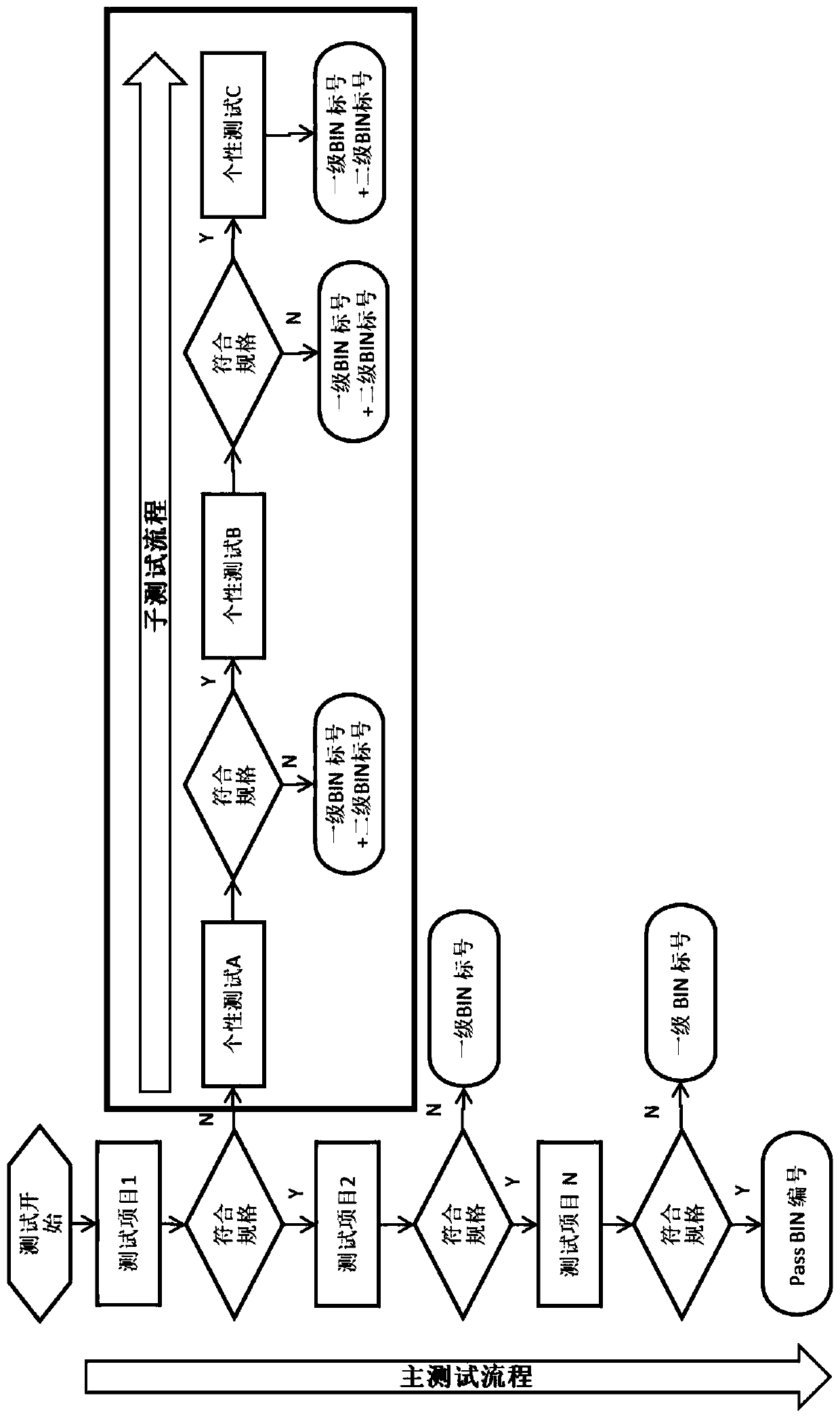
[0028] The wafer testing method described in the present invention adds secondary testing items to the traditional testing process. The present invention uses a test probe machine to test the chips on the wafer, and the test program includes a main test process and a sub-test process:

[0029] The main test process, that is, the traditional wafer probe test process, includes several first-level bin test items such as test items 1 to N, and the wafers are tested sequentially according to the first-level bin test items. Such as figure 2 As shown, in the main test process, the test of test item 1 is carried out first. After obtaining the test result of test item 1, if the test result is qualified, then enter the next level of test items to continue the test of the main test process; if the test If the result shows that it is invalid, it can enter the sub-test process.

[0030] The sub-test process forms a second-level test item, including several personality test items, which ...


PUM


Abstract

The invention discloses a wafer testing method, and a testing program of the wafer testing method comprises a main testing process and a sub-testing process. The main testing process comprises a plurality of first-level sub-Bin testing items such as testing items 1-N, and the wafers are sequentially tested according to the first-level sub-Bin testing items. The sub-testing process comprises a plurality of individual testing items, and the individual testing items are failure diagnosis testing items under the first-level sub-Bin testing items; the main testing process is used for quickly screening the wafers; and a sub-testing process entering the level is selected according to a testing item result of the main testing process, and a second-level sub-Bin label is output by the sub-testing process after the testing is completed. According to the invention, the second-level sub-testing process is added after the first-level main testing process, the chip after the first-level testing process can be further subjected to personalized testing, more chip testing data can be obtained, more failure information can be obtained, and meanwhile, testing items can be increased to the greatest extent to carry out more thorough testing on the wafer.

Description

technical field [0001] The invention relates to the field of manufacturing and testing of semiconductor devices, in particular to a wafer testing method. Background technique [0002] In the semiconductor device manufacturing process, testing is an important link to ensure the quality of the device when it leaves the factory. Through testing, some defective products or products with unqualified performance can be selected out during the manufacturing process, or the performance parameters of the device can be obtained through testing. , can classify products. [0003] Probe test (CP) is a very important test item in silicon wafer test. Probe test uses a probe card to contact the pads (PAD) on the wafer to transmit electrical signals. The probe card is the interface between the test instrument and the device under test (DUT). A typical probe card is a printed circuit board with many fine needles, which are physically and electrically connected to the device under test. In c...

Claims


Application Information

Patent Timeline
IPC IPC(8): H01L21/66
CPCH01L22/10
Inventor 吴苑
Owner SHANGHAI HUAHONG GRACE SEMICON MFG CORP
Why Eureka
Try Eureka