Eureka AIR delivers breakthrough ideas for toughest innovation challenges, trusted by R&D personnel around the world.

Photoelectric composite data bus and preparation method thereof

A data bus and photoelectric composite technology, which is applied in cable/conductor manufacturing, circuit, optics, etc., can solve the problems that the photoelectric signals of the bus cannot be transmitted at the same time, are not resistant to low temperature, and are not resistant to high temperature, and achieve good photoelectric transmission performance.

Pending Publication Date: 2020-05-12
西安飞机工业(集团)亨通航空电子有限公司
View PDF0 Cites 0 Cited by
  • Summary
  • Abstract
  • Description
  • Claims
  • Application Information

AI Technical Summary

Problems solved by technology

[0003] In order to solve the problem that the photoelectric signal of the bus in the prior art cannot be transmitted at the same time and is not resistant to high temperature or low temperature, the present invention discloses a photoelectric composite data bus and its preparation method, which can meet other basic electrical and mechanical properties At the same time as the index requirements, it can also meet the requirements that the bus can transmit photoelectric signals at the same time, and can withstand high and low temperatures from -65°C to +200°C. It can meet the technical effect of transmitting photoelectric multiplex signals in aerospace vehicle missions and control systems.

Method used


Image

  • Photoelectric composite data bus and preparation method thereof
  • Photoelectric composite data bus and preparation method thereof
  • Photoelectric composite data bus and preparation method thereof

Examples


Embodiment 1

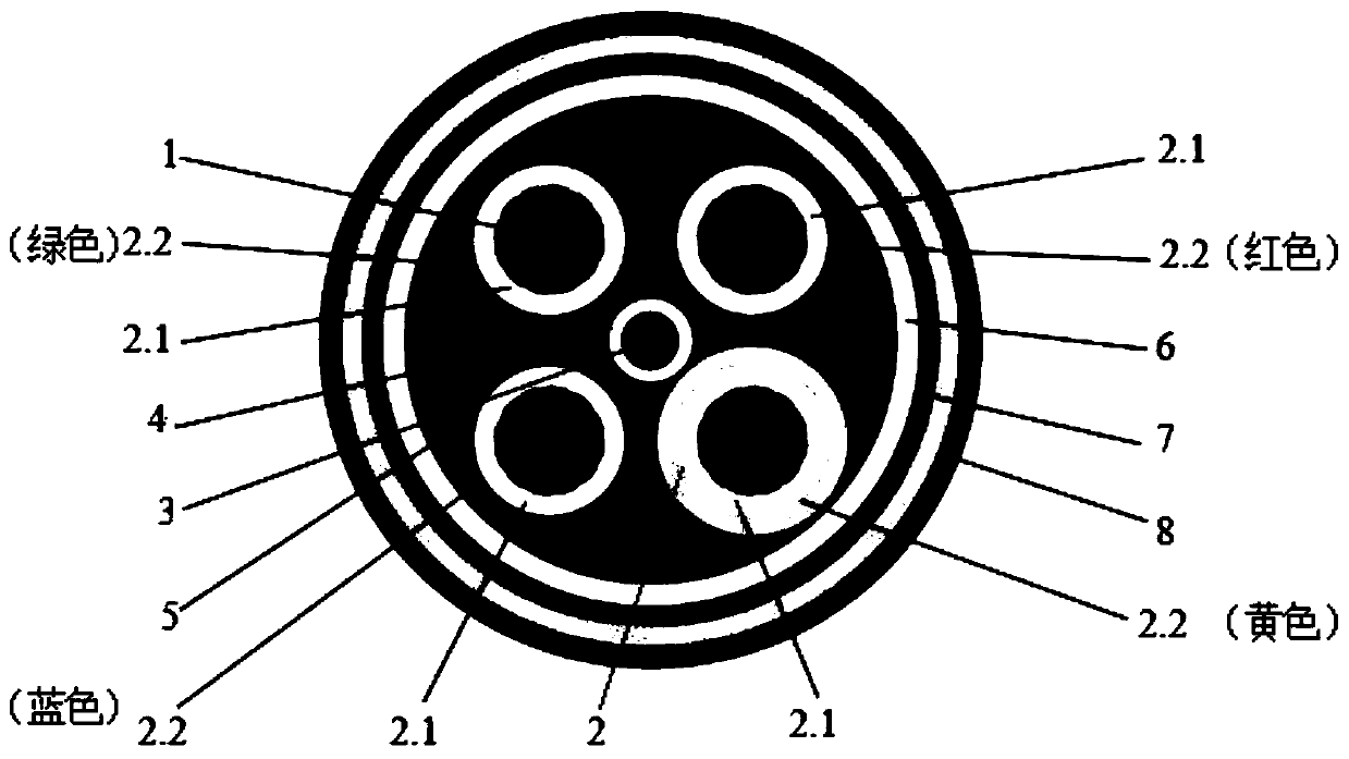
[0043] Embodiment 1, in conjunction with attached figure 1 describe.

[0044] An optoelectronic composite data bus, characterized in that it includes at least three silver-plated copper wire stranded conductors 1 and a single-mode optical fiber transmission carrier 3; the silver-plated copper wire stranded conductor 1 is wrapped with a first insulating layer 2; The single-mode optical fiber transmission carrier 3 is wrapped with a second insulating layer 4; the outer circumferential direction of the single-mode optical fiber transmission carrier 3 is stranded with the silver-plated copper wire stranded conductor 1 to form a photoelectric composite cable core 5; The photoelectric composite cable core 5 is wrapped with a fastening layer 6; the fastening layer 6 is provided with a shielding layer 7;

[0045] The optoelectronic composite data bus of this embodiment uses three silver-plated copper wire stranded conductors for electrical signal transmission and a single-mode optica...

Embodiment 2

[0051] Embodiment 2, in conjunction with attached figure 1 describe.

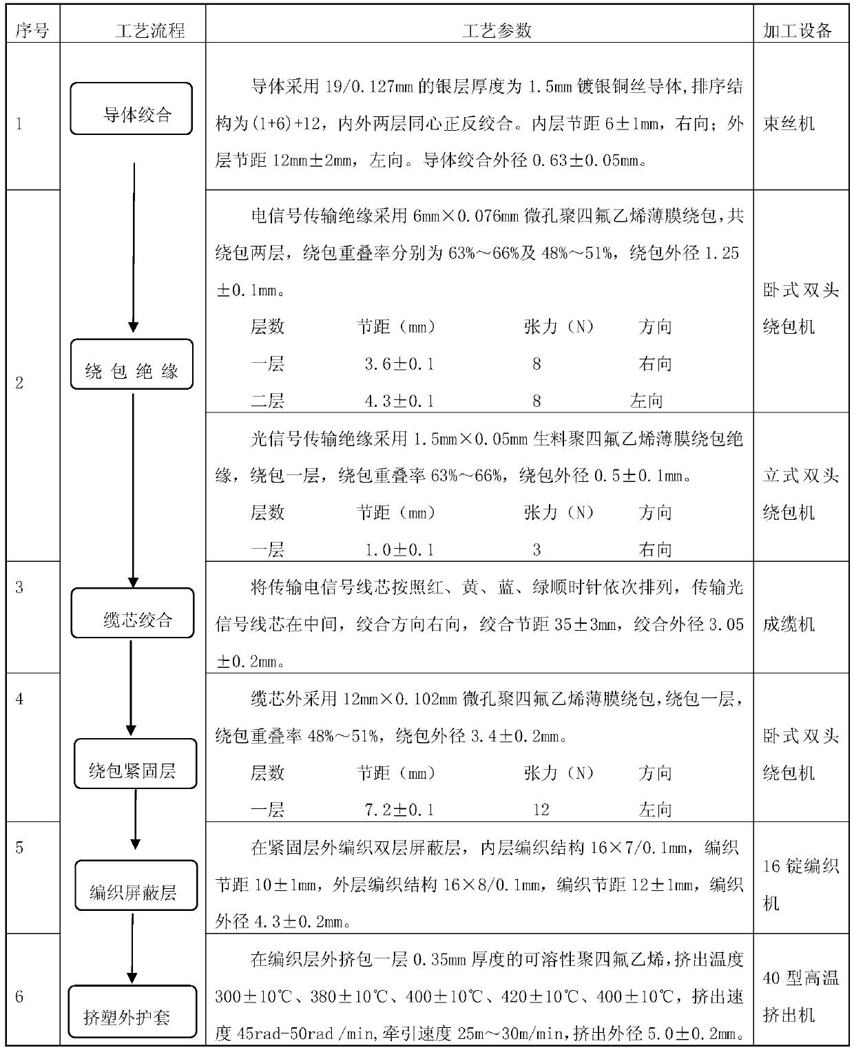
[0052] For further clarifying the technical effect of the photoelectric composite data bus of the present invention, a kind of method for preparing the product of embodiment 1 is provided:

[0053] A preparation method for an optoelectronic composite data bus, specifically comprising the steps of:

[0054] Step 1. Preparation of silver-plated copper wire stranded conductor 1: Arrange single conductors in sequence from the inside to the outside with a bundle machine, and twist out the silver-plated copper wire conductors from the inside to the outside in forward and reverse directions;

[0055] Step 2. Wrapping the first insulating layer 2: Wrap the silver-plated copper wire stranded conductor 1 with a microporous polytetrafluoroethylene film with a width of 6mm x a thickness of 0.076mm by a horizontal double-headed wrapping machine, and wrap two layers in total to form first insulating layer 2;

[0056] ...

Embodiment 3

[0070] Embodiment 3, in conjunction with attached figure 1 describe.

[0071] For further clarifying the technical effect of the photoelectric composite data bus of the present invention, a kind of method for preparing the product of embodiment 1 is provided:

[0072] A preparation method for an optoelectronic composite data bus, specifically comprising the steps of:

[0073] Step 1. Preparation of silver-plated copper wire stranded conductor 1: Arrange single conductors in sequence from the inside to the outside with a bundle machine, and twist out the silver-plated copper wire conductors from the inside to the outside in forward and reverse directions;

[0074] Step 2. Wrapping the first insulating layer 2: Wrap the silver-plated copper wire stranded conductor 1 with a microporous polytetrafluoroethylene film with a width of 6mm x a thickness of 0.076mm by a horizontal double-headed wrapping machine, and wrap two layers in total to form first insulating layer 2;

[0075] ...


PUM

PropertyMeasurementUnit
Tensile strengthaaaaaaaaaa
Diameteraaaaaaaaaa
Thicknessaaaaaaaaaa

Abstract

The invention discloses a photoelectric composite data bus and a preparation method thereof. The photoelectric composite data bus comprises at least three silver-plated copper wire stranded conductorsand a single-mode optical fiber transmission carrier; the silver-plated copper wire stranded conductors are wrapped with a first insulating layer; the single-mode optical fiber transmission carrier is wrapped by a second insulating layer; the silver-plated copper wire stranded conductors are stranded in the peripheral direction of the single-mode optical fiber transmission carrier to form a photoelectric composite cable core; a fastening layer is disposed outside the photoelectric composite cable core in a wrapping manner; a shielding layer is arranged outside the fastening layer; an outer sheath is extruded outside the shielding layer, and the photoelectric composite data bus is obtained through the method of twisting the conductors, wrapping the insulating layer, forming the electric composite cable core, wrapping the fastening layer and the shielding layer, and extruding the outer sheath. According to the invention, the problems that photoelectric signals cannot be transmitted at the same time and are not resistant to high temperature and low temperature are solved, and the technical effects that the bus can transmit the photoelectric signals at the same time, can resist high and low temperatures of-65 DEG C to + 200 DEG C, and can meet the requirement for transmitting photoelectric multi-path signals in aerospace craft tasks and control systems are achieved.

Description

technical field [0001] The invention relates to the technical field of signal transmission cables for aerospace, in particular to a photoelectric composite data bus and a preparation method thereof. Background technique [0002] The photoelectric data bus is a high-speed serial bus and optical fiber channel transmission carrier. In the development process of my country's new stealth fighter, it will also use the photoelectric composite data bus communication interface to transmit complex, diverse and efficient video and image signals. ; Develop this type of photoelectric composite data bus, so that the photoelectric composite data bus can also meet other harsh military environments such as field operations and water surfaces within a wide temperature range. However, in the existing bus signal transmission, one is that the photoelectric signals cannot be transmitted in the same way at the same time, and the other is that the optical signals are not resistant to high temperatur...

Claims


Application Information

Patent Timeline
IPC IPC(8): H01B11/22H01B1/02H01B3/44H01B7/02H01B7/04H01B7/17H01B7/28H01B7/29H01B13/02H01B13/08H01B13/24H01B13/26G02B6/44
CPCG02B6/443G02B6/4486H01B1/026H01B3/445H01B7/02H01B7/04H01B7/17H01B7/28H01B7/29H01B11/22H01B13/02H01B13/08H01B13/24H01B13/2606
Inventor 余小葵纪宏生陈参波崔闫雪李莎杨拓
Owner 西安飞机工业(集团)亨通航空电子有限公司
Why Eureka
Eureka Blog
Learn More