
DDR SDRAM physical layer interface circuit and DDR SDRAM control device

A physical layer interface, physical layer technology, applied in the direction of electrical digital data processing, data processing input/output process, static memory, etc., can solve the problems of long delay of the clock tree and difficult timing convergence.

Active Publication Date: 2020-05-15
REALTEK SEMICON CORP
View PDF9 Cites 2 Cited by
  • Summary
  • Abstract
  • Description
  • Claims
  • Application Information

AI Technical Summary

Problems solved by technology

[0002] With the evolution of Double Data Rate Synchronous Dynamic Random Access Memory (DDR SDRAM) technology, the applicant proposed in US Patent No. 9,570,130B2 to use a delay-locked loop (delay-locked loop, DLL) to handle high-speed DDR SDRAM applications. Timing is not easy to converge and the clock tree latency is too long

Method used


Image

  • DDR SDRAM physical layer interface circuit and DDR SDRAM control device
  • DDR SDRAM physical layer interface circuit and DDR SDRAM control device
  • DDR SDRAM physical layer interface circuit and DDR SDRAM control device

Examples


Embodiment Construction

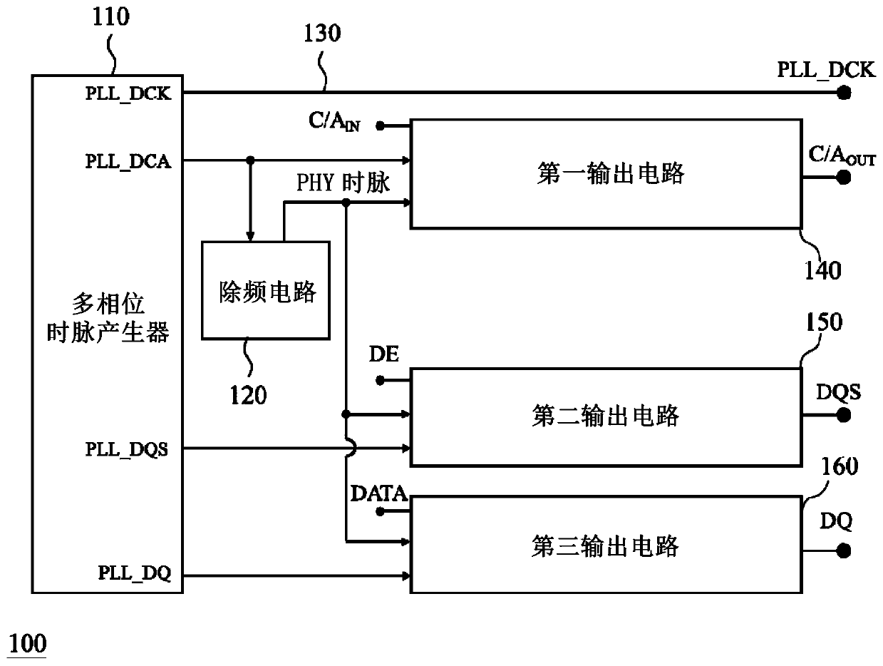
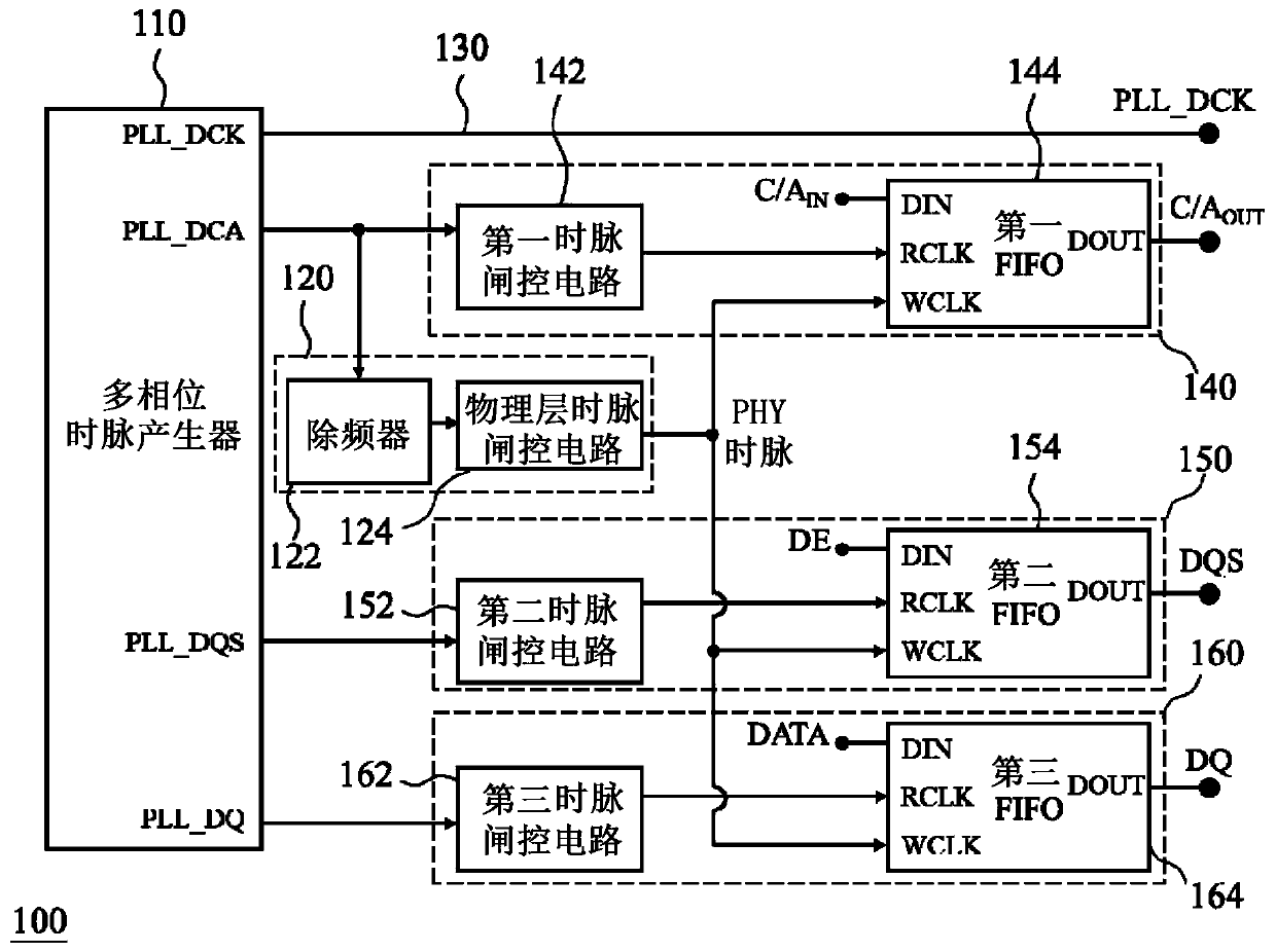
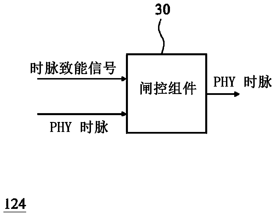
[0019] The invention discloses a double data rate synchronous dynamic random access memory (DDR SDRAM) physical layer interface circuit and a DDR SDRAM control device. Compared with the invention of the applicant's patent (US 9,570,130B2), the DDR SDRAM physical layer interface circuit and the DDR SDRAM control device of the present invention have the advantages of smaller circuit area and / or less power consumption. It should be noted that those skilled in the art can refer to this US patent (US 9,570,130B2) to understand the background knowledge of the present invention.

[0020] figure 1 An embodiment of the DDR SDRAM physical layer interface circuit of the present invention is shown, which can be used to adjust the phase of a signal between a memory controller and a storage circuit without using a delay locked loop that consumes a large amount of circuit area. figure 1 The DDR SDRAM physical layer interface circuit 100 comprises a multi-phase clock generator 110, a frequen...


PUM


Abstract

The invention provides a DDR SDRAM physical layer interface circuit and a DDR SDRAM control device. Disclosed is a DDR SDRAM physical layer interface circuit that uses less circuit area and can adjustthe phase of the signal between a memory controller and a storage circuit, the DDR SDRAM physical layer interface circuit including: a multiphase clock generator generating a plurality of clocks including a reference clock, a first clock, a second clock and a third clock; a frequency dividing circuit generating a PHY clock according to the first clock; a clock output path outputting the referenceclock to a storage circuit; a first output circuit outputting a first output signal to the storage circuit according to a first input signal of a memory controller, the first clock and the PHY clock;a second output circuit outputting a second output signal to the storage circuit according to a second input signal of the memory controller, the second clock and the PHY clock; and a third output circuit outputting a third output signal to the storage circuit according to a third input signal of the memory controller, the third clock and the PHY clock.

Description

technical field [0001] The present invention relates to a double data rate synchronous dynamic random access memory (DDR SDRAM) physical layer interface circuit and a DDR SDRAM control device, in particular to a DDR SDRAM physical layer interface circuit with smaller circuit area and / or less power consumption with DDR SDRAM control device. Background technique [0002] With the evolution of Double Data Rate Synchronous Dynamic Random Access Memory (DDR SDRAM) technology, the applicant proposed in US Patent No. 9,570,130B2 to use a delay-locked loop (delay-locked loop, DLL) to handle high-speed DDR SDRAM applications. Timing is not easy to converge and the clock tree latency is too long. However, the applicant believes that there is room for further improvement in terms of the circuit area and energy saving of the above-mentioned prior art. Contents of the invention [0003] An object of the present invention is to provide a double data rate synchronous dynamic random acc...

Claims


Application Information

Patent Timeline
IPC IPC(8): G11C7/10G11C7/22G11C11/4093G11C11/4096
CPCG11C7/1057G11C7/1084G11C7/22G11C11/4093G11C11/4096G06F13/1689G11C7/1093G11C7/222G11C2207/2254Y02D10/00G06F3/0604G06F3/0656G06F3/0659G06F3/0673G11C7/225
Inventor 纪国伟余俊锜张志伟周格至陈世昌
Owner REALTEK SEMICON CORP
Features
  • Generate Ideas
  • Intellectual Property
  • Life Sciences
  • Materials
  • Tech Scout
  • Unparalleled Data Quality
  • Higher Quality Content
  • 60% Fewer Hallucinations
Learn More