Eureka AIR delivers breakthrough ideas for toughest innovation challenges, trusted by R&D personnel around the world.

NOR FLASH chip and method for eliminating over-erasing in erasing process of NOR FLASH chip

An over-erasing and chip technology, which is applied in the field of NORFLASH chip and eliminates over-erasing in its erasing process, can solve the problem of non-volatile memory such as long time

Active Publication Date: 2020-05-22
XTX TECH INC
View PDF9 Cites 5 Cited by
  • Summary
  • Abstract
  • Description
  • Claims
  • Application Information

AI Technical Summary

Problems solved by technology

However, the solution is carried out during the power-on process, which leads to a long time for the power-on process of the non-volatile memory

Method used


Image

  • NOR FLASH chip and method for eliminating over-erasing in erasing process of NOR FLASH chip
  • NOR FLASH chip and method for eliminating over-erasing in erasing process of NOR FLASH chip
  • NOR FLASH chip and method for eliminating over-erasing in erasing process of NOR FLASH chip

Examples


Embodiment Construction

[0033] It should be understood that the specific embodiments described here are only used to explain the present invention, not to limit the present invention.

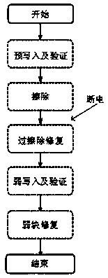
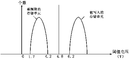
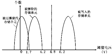
[0034] refer to figure 2 , figure 2 It is a schematic diagram of the relationship between the erased and written memory cells and the threshold voltage in the NOR FLASH chip. Such as figure 2 As shown, under normal circumstances, the memory cells in the NOR FLASH chip include erased memory cells (threshold voltage 1.7v~4.2v) and written memory cells (threshold voltage above 6.2v). When the chip is power-off during the erasing process, for example, the power-off occurs at the stage before erasing and repairing the target block after erasing the target block, and some memory cells will be erased. The phenomenon of over-erasing will occur, and the threshold voltage of some of these over-erased memory cells will be less than 0v, which will cause the read operation after NOR FLASH is powered on again, because of the ...


PUM


Abstract

The invention provides an NOR FLASH chip and a method for eliminating over-erasing in an erasing process of the NOR FLASH chip. The method comprises the following steps: when an erasing command is received for the first time after an NOR FLASH chip is powered on, over-erasing repair and weak write-in and verification operations are carried out on storage blocks of the whole NOR FLASH chip, and anoriginal erasing process continues to be completed after the over-erasing repair and weak write-in and verification operations on all the storage blocks are completed. According to the NOR FLASH chip,due to the fact that all the storage blocks are subjected to over-erasing repair and weak write-in and verification operations, an over-erased storage unit does not exist in the NOR FLASH chip any more. Therefore, when a read operation is encountered, the situation that read data is wrong due to the existence of the over-erased storage unit is avoided.

Description

technical field [0001] The invention relates to the technical field of semiconductor memory, in particular to a NOR FLASH chip and a method for eliminating over-erasing during its erasing process. Background technique [0002] The NORFLASH chip is a non-volatile flash memory chip, and its erasing process is to pre-write all the bits in the target erasing block to 0, and then perform the erasing operation on the target erasing block. After the erasing is completed, operations such as erasure repair, weak write and verification, and weak block repair are performed. This series of operations forms a complete erasing process, the process is as follows figure 1 shown. figure 1 A schematic diagram of the existing erasing process. [0003] However, in the actual application process, it is likely to encounter the problem of power failure during the erasing process, so that a complete erasing process cannot be completed. If the power-off occurs at the stage before the over-erase ...

Claims


Application Information

Patent Timeline
Patent Type & Authority Applications(China)
IPC IPC(8): G11C16/16G11C16/34G11C29/44
CPCG11C16/16G11C16/3409G11C29/44
Inventor 王文静于文贤张涌
Owner XTX TECH INC
Why Eureka
Eureka Blog
Learn More