Wavy pattern of integrated circuit and method of forming same, integrated circuit

An integrated circuit and wave-shaped technology, which is applied in the manufacture of circuits, electrical components, semiconductors/solid-state devices, etc., can solve the problems of broken wires in wave-shaped patterns, small k1 values, and reduced yields of integrated circuit manufacturing, so as to improve manufacturing yields. rate, reducing the effect of disconnection

Active Publication Date: 2022-03-08
CHANGXIN MEMORY TECH INC
View PDF5 Cites 0 Cited by
  • Summary
  • Abstract
  • Description
  • Claims
  • Application Information

AI Technical Summary

Problems solved by technology

[0004] In related technologies, one-time patterning process is usually used to process wavy patterns, but in order to ensure good resolution, the value of k1 is usually small, so when using one-time patterning process to process wavy patterns, it is easy to appear at the bend of the wavy pattern. The case of disconnection reduces the manufacturing yield of integrated circuits

Method used


Image

  • Wavy pattern of integrated circuit and method of forming same, integrated circuit
  • Wavy pattern of integrated circuit and method of forming same, integrated circuit
  • Wavy pattern of integrated circuit and method of forming same, integrated circuit

Examples


Embodiment Construction

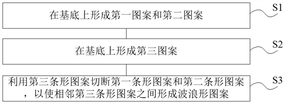
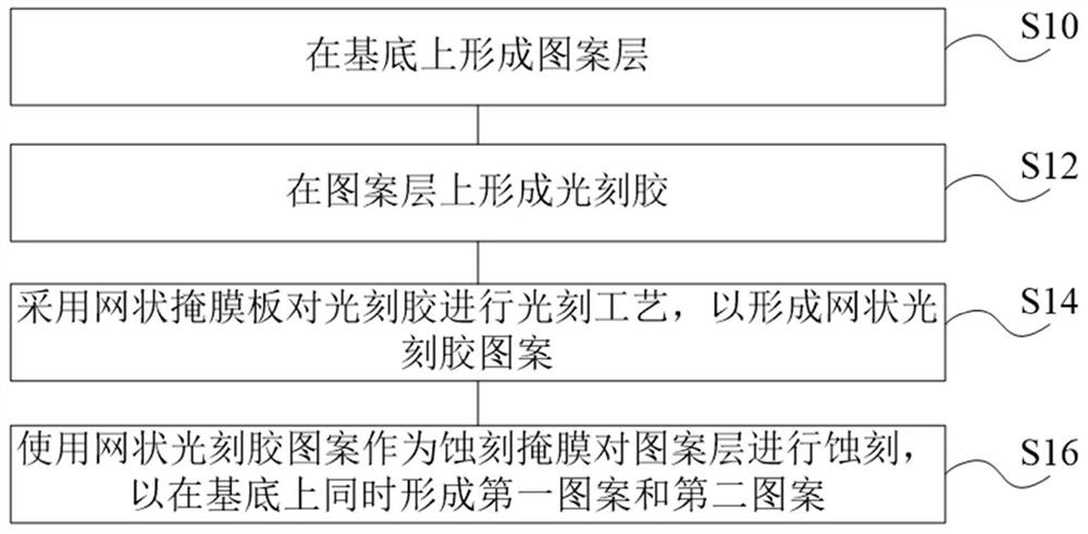
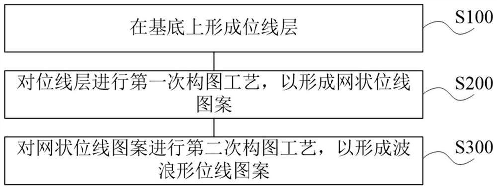
[0046] Example embodiments will now be described more fully with reference to the accompanying drawings. Example embodiments may, however, be embodied in many forms and should not be construed as limited to the embodiments set forth herein; rather, these embodiments are provided so that this application will be thorough and complete, and will fully convey the concept of example embodiments to those skilled in the art. The same reference numerals in the drawings denote the same or similar structures, and thus their detailed descriptions will be omitted.

[0047] Although relative terms such as "upper" and "lower" are used in this specification to describe the relative relationship of one component of an icon to another component, these terms are used in this specification only for convenience, for example, according to the description in the accompanying drawings directions for the example described above. It will be appreciated that if the illustrated device is turned over s...


PUM


Abstract

The present application relates to the technical field of semiconductor fabrication, and in particular, to a method for forming a wavy pattern of an integrated circuit, a wavy pattern of an integrated circuit, and an integrated circuit, wherein the method for forming the wavy pattern includes: forming a wavy pattern on a substrate The first pattern and the second pattern, the first pattern includes a plurality of first bar-shaped patterns arranged at intervals in the first direction, and the second pattern includes a plurality of first bar-shaped patterns arranged at intervals in the second direction and connected to the first bar-shaped pattern Intersecting second strip pattern; forming a third pattern on the substrate, the third pattern is located on the first pattern and the second pattern, and the third pattern includes a plurality of spaced in the third direction and is arranged with the first strip pattern and the second pattern. The third bar pattern where the second bar pattern intersects; the first bar pattern and the second bar pattern are cut off by using the third bar pattern, so that a wavy pattern is formed between adjacent third bar patterns. Such a design can reduce the disconnection of the wavy pattern and improve the manufacturing yield of the integrated circuit.

Description

technical field [0001] The present application relates to the technical field of semiconductor manufacturing, in particular, to a method for forming a wave-shaped pattern of an integrated circuit, a wave-shaped pattern of an integrated circuit, and the integrated circuit. Background technique [0002] With the development of integrated circuit manufacturing, the integration level is getting higher and higher, and the number of transistors contained in a unit area is also increasing rapidly. The main index to measure the degree of integration in the manufacturing process is the resolution of the photolithography process, which is used to distinguish the ability of the feature pattern close to the surface of the silicon wafer. [0003] Currently, the resolution R is generally measured by a critical dimension (CD, Critical Dimension). Wherein, the smaller the critical dimension formed, the better the resolution. In order to obtain a smaller critical dimension, it can be impro...

Claims


Application Information

Patent Timeline
Patent Type & Authority Patents(China)
IPC IPC(8): H01L21/027H01L21/3213
CPCH01L21/0271H01L21/32139
Inventor 不公告发明人
Owner CHANGXIN MEMORY TECH INC
Why Eureka
Try Eureka