Time domain finite difference method hardware accelerator architecture and implementation method thereof

A technology of finite difference in time domain and hardware accelerator, which is applied to architectures, instruments, and digital computer components with a single central processing unit. and other problems, to achieve the effect of correct function, play off-chip storage bandwidth capacity, and improve utilization rate

Active Publication Date: 2020-05-29
SUN YAT SEN UNIV
View PDF7 Cites 1 Cited by
  • Summary
  • Abstract
  • Description
  • Claims
  • Application Information

AI Technical Summary

Problems solved by technology

This defect will cause different projects to be simulated each time to re-program the FPGA bit stream to configure hardware accelerators with different architectures. The amount of engineering is very large, and it is difficult to be practical in actual projects.
That is, the scalability and grid adaptability of the PE array are very weak

Method used


Image

  • Time domain finite difference method hardware accelerator architecture and implementation method thereof
  • Time domain finite difference method hardware accelerator architecture and implementation method thereof
  • Time domain finite difference method hardware accelerator architecture and implementation method thereof

Examples


Embodiment Construction

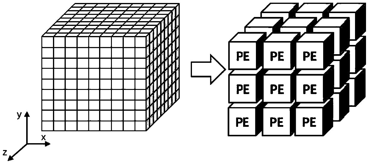
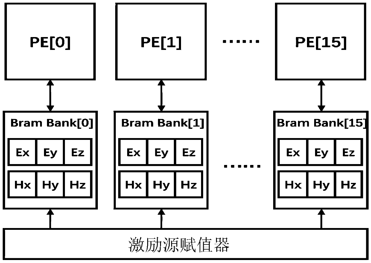
[0041] Such as figure 1 As shown, when the existing FDTD hardware accelerator based on the FPGA (Field Programmable Gate Array) platform calculates the electromagnetic field in the three-dimensional space, the large grid that needs to be simulated will be based on the logical resources and storage resources on the FPGA. The number of small grids is evenly divided into several small grids, and each small grid is allocated a computing processing unit PE (Processing Element) and a set of BRAM (Block RAM) for storing data, forming a three-dimensional array of small grids . Each PE is responsible for calculating the electric field value and magnetic field value of all grid points in the small grid, and updating the value of each grid point in turn by scanning. After all the small grids are calculated, the electric field value and magnetic field value in the small grid BRAM are output according to the combination of small grids to restore the structure of the large grid.

[0042]W...


PUM


Abstract

The invention discloses a time domain finite difference method hardware accelerator architecture. The architecture comprises a chain type calculation processing unit arrangement structure, multiple groups of storage blocks and an excitation source assignment device, the arrangement structure of the chained calculation processing unit is a combination of a plurality of PE arranged in the one-dimensional direction and is used for calculating the electric field value and/or the magnetic field value of the three-dimensional grid points simulated by the electromagnetic field; the storage block is composed of a plurality of block random access memories and is used for storing the electric field values and/or the magnetic field values of the grid points calculated by the PE; and the excitation source valuator is used for valuating the electric field value and/or the magnetic field value stored in the storage block. According to the invention, the utilization rate of the PE can be improved, the wiring difficulty and time delay comprehensively realized on the FPGA are reduced, the off-chip storage bandwidth capability is increased, and the expansibility and grid adaptability of the PE arrayare improved. The method can be applied to the field of hardware accelerators based on FPGA platforms.

Description

technical field [0001] The invention relates to the field of a hardware accelerator based on an FPGA platform, in particular to a time domain finite difference method hardware accelerator architecture and an implementation method thereof. Background technique [0002] When the existing FDT hardware accelerator based on the FPGA (Field Programmable Gate Array) platform calculates the electromagnetic field in three-dimensional space, the large grid that needs to be simulated will be calculated according to the logic resources and storage resources on the FPGA. Evenly divided into several small grids, and each small grid is allocated a computing processing unit PE (Processing Element) and a set of block random access memory BRAM (Block RAM) for storing data, forming a three-dimensional array of small grids . Each calculation processing unit PE is responsible for calculating the electric field value and magnetic field value of all grid points in the small grid, and updating the...

Claims


Application Information

Patent Timeline
Patent Type & Authority Applications(China)
IPC IPC(8): G06F15/78
CPCG06F15/7896
Inventor 粟涛孔昶陈弟虎
Owner SUN YAT SEN UNIV
Why Eureka
Try Eureka