Method for manufacturing semiconductor device

A semiconductor and device technology, applied in the field of manufacturing semiconductor devices

Pending Publication Date: 2020-05-29
INFINEON TECH AG
View PDF0 Cites 2 Cited by
  • Summary
  • Abstract
  • Description
  • Claims
  • Application Information

AI Technical Summary

Problems solved by technology

Followed by one or more proton injections

Method used


Image

  • Method for manufacturing semiconductor device
  • Method for manufacturing semiconductor device
  • Method for manufacturing semiconductor device

Examples


Embodiment Construction

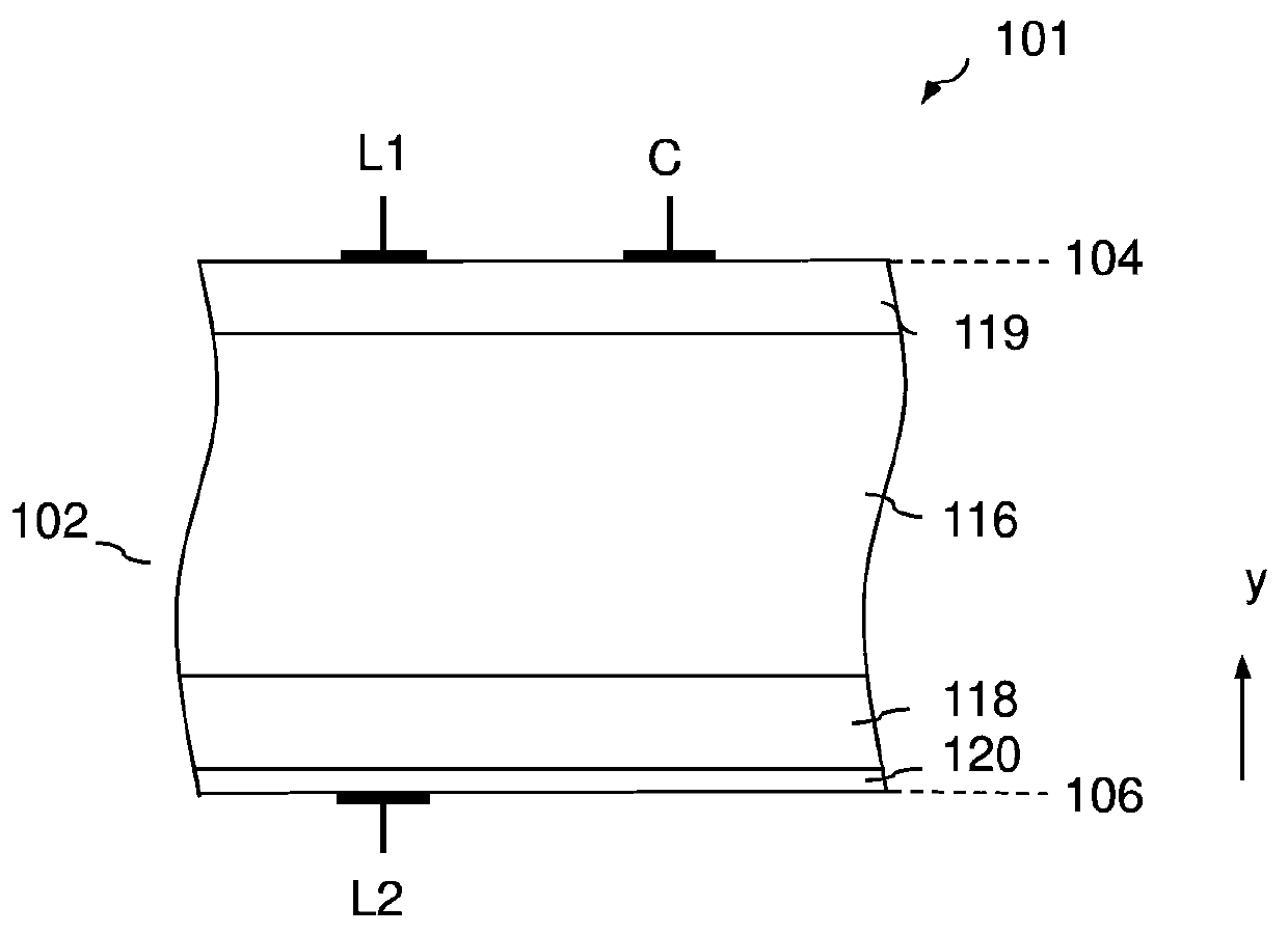
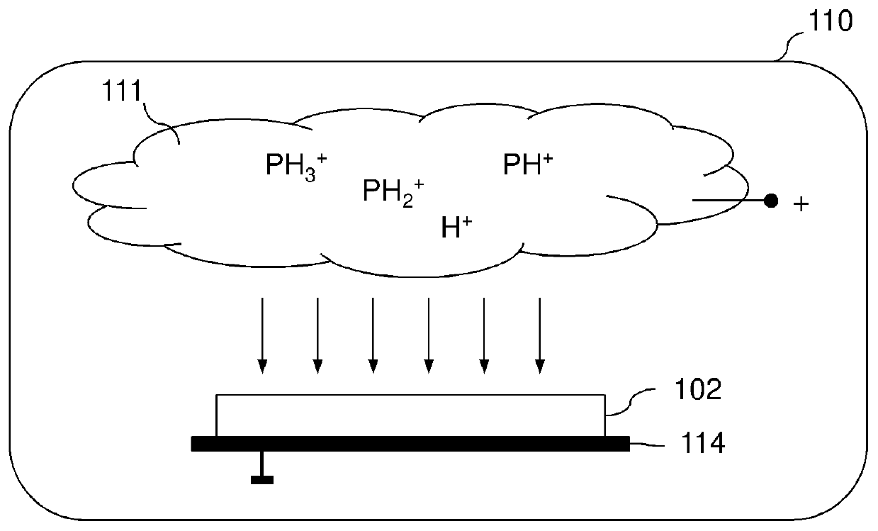
[0013] In the following detailed description, reference is made to the accompanying drawings, which form a part of this disclosure, and in which are shown certain embodiments for purposes of illustration. In this context, directional terms such as "upper side", "bottom", "front", "rear", "front", "rear", etc. refer to the orientation of the drawings just described. Since components of the embodiments may be positioned in different orientations, directional terms are used for illustration only and should in no way be construed as limiting.

[0014] It goes without saying that other embodiments exist and that structural or logical changes may be made to the embodiments without departing from the scope defined by the claims. The description of the embodiments is not limiting in this respect. In particular, elements of the embodiments described below may be combined with elements of other embodiments in the described embodiments, unless the context dictates otherwise.

[0015] H...


PUM


Abstract

The present disclosure relates to a method for manufacturing a semiconductor device. The method includes introducing at least one first dopant into a semiconductor body (102) through a first surface (104) of the semiconductor body (102). One or more proton implants are then performed. The method also includes introducing a second dopant into the semiconductor body (102) through a second surface (106) opposite the first surface (104) using a plasma-based ion implantation method, wherein the plasma-based ion implantation method is carried out using a composite of the second dopant and hydrogen as a process gas.

Description

technical field [0001] The present application relates to a method for manufacturing a semiconductor device. Background technique [0002] When manufacturing semiconductor devices, such as power semiconductor devices such as insulated gate bipolar transistors (IGBTs) or power diodes, it is necessary to accept a compromise in terms of the desired device characteristics, as changes in, for example, device parameters may have differences in the device characteristics effects, such as may result in an improvement of one device characteristic while degrading another, or the technology on which semiconductor device fabrication is based may also result in limitations in wafer processing, for example when dealing with thin or thinned wafers time limit. Against this background, the present application is directed to improvements in methods of fabricating semiconductor devices. Contents of the invention [0003] The present disclosure relates to a method for manufacturing a semico...

Claims


Application Information

Patent Timeline
Patent Type & Authority Applications(China)
IPC IPC(8): H01L21/331H01L21/265
CPCH01L21/26513H01L29/66333H01L21/2236H01L21/26506H01L29/0873H01L29/36H01L29/7395H01L29/74H01L29/7802H01L29/861
Inventor H-J.舒尔策M.耶利内克A.毛德T.韦本
Owner INFINEON TECH AG
Why Eureka
Try Eureka