3D NAND memory and manufacturing method thereof

A 3D NAND and manufacturing method technology, applied in the direction of electric solid-state devices, semiconductor devices, electrical components, etc., can solve the problems of limited grid line gap size, affecting the use of devices, leakage, etc., to facilitate formation, reduce time, and reduce production costs Effect

Active Publication Date: 2020-06-02
YANGTZE MEMORY TECH CO LTD
View PDF4 Cites 9 Cited by
  • Summary
  • Abstract
  • Description
  • Claims
  • Application Information

AI Technical Summary

Problems solved by technology

[0003] In the 3D NAND process, gate line gaps are usually formed to form stacked gate layers. In order to control the effective gate area, the size of the gate line gaps needs to be limited, thus making the size of the gate line gaps very limited. When the common source is subsequently formed through the gate line

Method used


Image

  • 3D NAND memory and manufacturing method thereof
  • 3D NAND memory and manufacturing method thereof
  • 3D NAND memory and manufacturing method thereof

Examples


Embodiment 1

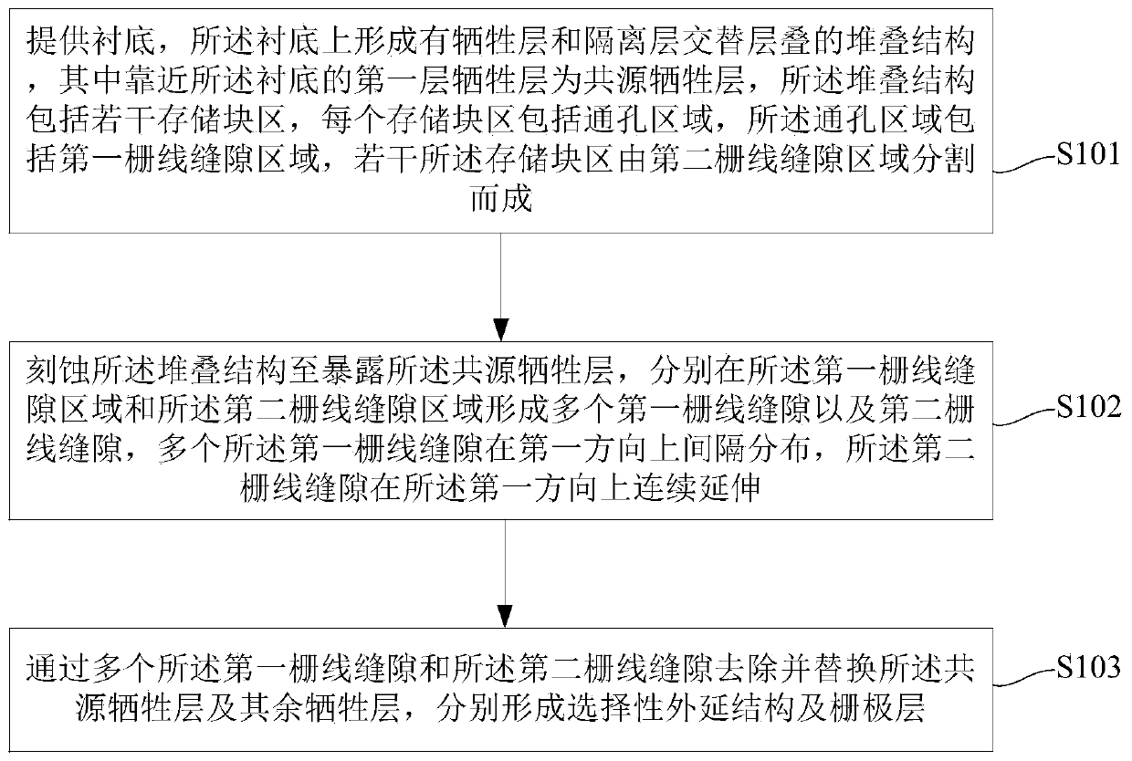
[0095] This embodiment provides a method for manufacturing a 3D NAND memory, such as image 3 As shown, the method includes the following steps:

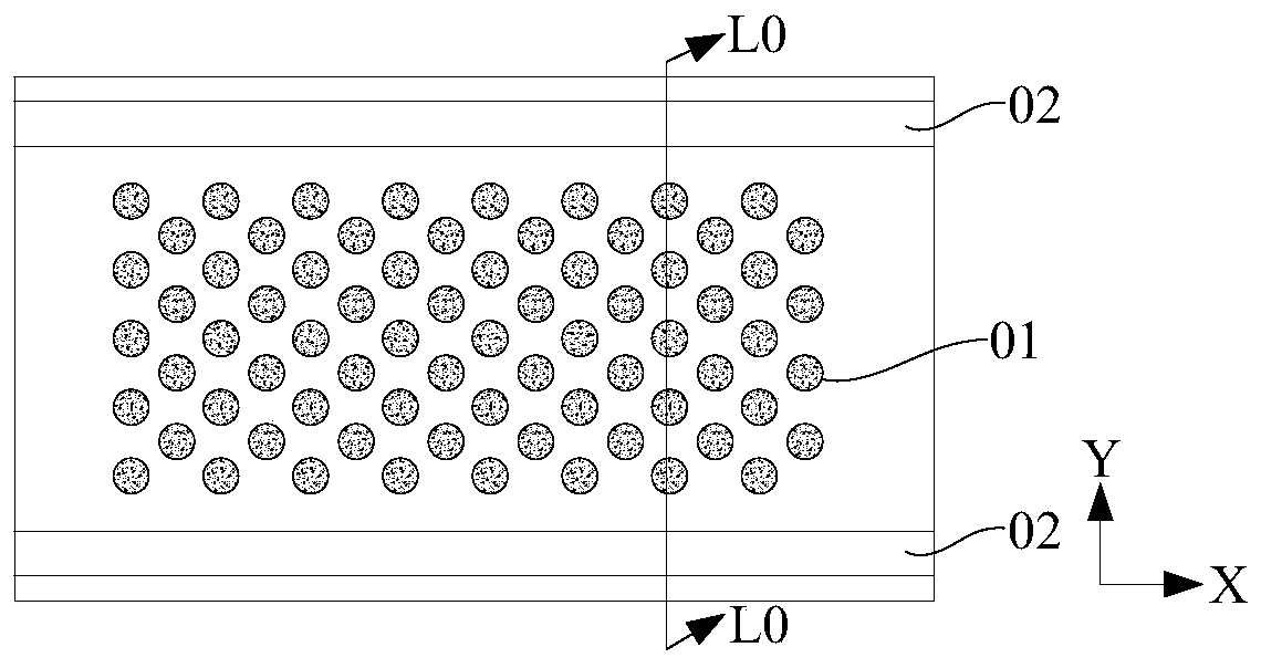
[0096] Step S101: Provide a substrate, on which a stack structure of alternately stacked sacrificial layers and isolation layers is formed, wherein the first sacrificial layer close to the substrate is a common-source sacrificial layer, and the stack structure includes several storage Block areas, each memory block area includes a through hole area, the through hole area includes a first gate line gap area, and several memory block areas are divided by the second gate line gap area;

[0097] Provide a substrate 100, the material of the substrate 100 can be single crystal silicon (Si), single crystal germanium (Ge), or silicon germanium (GeSi), silicon carbide (SiC); it can also be silicon on insulator (SOI) , germanium on insulator (GOI); or other materials, such as III-V group compounds such as gallium arsenide. In this embodimen...

Embodiment 2

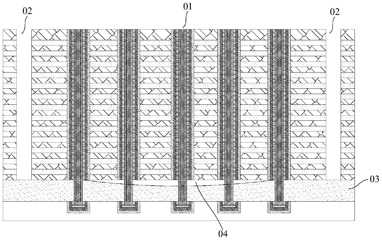
[0110] This embodiment provides a kind of 3D NAND memory, refer to the attached Figure 4 ~ attached Figure 17 , the 3D NAND memory includes:

[0111] A substrate 100, on which a stacked structure 101 is formed, the stacked structure is formed by alternating arrangement of gate layers 110 and isolation layers, and the stacked structure includes several memory blocks; in this embodiment, the gate conductive material can be It is a metal material, such as tungsten, etc.

[0112] A selective epitaxial structure 108 is formed between the substrate and the stack structure. The epitaxial structure 108 in this embodiment has a uniform structure without defects such as gaps, thereby avoiding risks such as electric leakage in the later stage of the device. as well as

[0113] A plurality of first array common sources formed in the storage block are distributed at intervals in the first direction.

[0114] In this embodiment, the material of the substrate 100 can be single crystal...


PUM


Abstract

The invention provides a 3D NAND memory and a manufacturing method thereof. The method comprises the steps of forming a stacked structure on a substrate, wherein the stacked structure comprises a storage block which is divided by a plurality of second grid line gaps continuously extending in the first direction, channel structures which are distributed in an array mode are formed in a through holearea of the storage block, first grid line gaps which extend in the first direction and are distributed at intervals are further formed in the through hole area of the storage block, and the first grid line gaps can be through holes formed in the middle of the channel structures of the through hole area. The first grid line gap is beneficial to the growth of an epitaxial structure near the innerrow channel structure in the through hole area, so that no gap exists near the inner row channel structure, and the risks of electric leakage and the like in the later period of the device are avoided. Besides, a sacrificial layer in the stacked structure is removed through the first grid line gap and the second grid line gap, so that the time required for removing the sacrificial layer can be remarkably reduced, the formation of a grid conductive material is facilitated at the same time, and the production cost can be correspondingly reduced.

Description

technical field [0001] The invention relates to the field of semiconductor integrated circuit manufacturing, in particular to a 3D NAND memory and a manufacturing method thereof. Background technique [0002] As the feature size of devices in integrated circuits continues to shrink, 3D memory technologies that stack multiple planes of memory cells to achieve greater storage capacity and lower cost per bit are increasingly favored. [0003] In the 3D NAND process, gate line gaps are usually formed to form stacked gate layers. In order to control the effective gate area, the size of the gate line gaps needs to be limited, thus making the size of the gate line gaps very limited. When the common source is subsequently formed through the gate line gap and the contact part of the common source is further formed, the position of the contact part and the common source is slightly deviated, which will cause the contact part to bridge the gate layers on both sides of the common source...

Claims


Application Information

Patent Timeline
IPC IPC(8): H01L27/1157H01L27/11578H01L27/11582
CPCH10B43/35H10B43/20H10B43/27H10B43/10Y02D10/00
Inventor 吴林春张坤
Owner YANGTZE MEMORY TECH CO LTD
Why Eureka
Try Eureka