
A two-dimensional horizontal homojunction, self-driven logic photoelectric switch and its preparation method

A photoelectric switch, homojunction technology, applied in electronic switches, circuits, electrical components, etc., can solve the problems of physical damage to materials, difficulty in ensuring interface cleanliness, affecting carrier transport performance, etc., to simplify the preparation process. Effect

Active Publication Date: 2022-04-05
UNIV OF SCI & TECH BEIJING
View PDF5 Cites 0 Cited by
  • Summary
  • Abstract
  • Description
  • Claims
  • Application Information

AI Technical Summary

Problems solved by technology

Traditional doping methods, such as ion implantation and surface modification, are difficult to form a stable doping state in 2D materials, while causing inevitable physical damage to the material
The p-n junction constructed by stacking method needs to be assisted by polymer film stacking, and it is difficult to ensure the cleanliness of the interface
In addition, due to the mechanical flexibility of 2D materials, uncontrollable random stacking and bubbles at the interface are difficult to completely resolve, which seriously affect the carrier transport performance of p-n junctions.

Method used


Image

  • A two-dimensional horizontal homojunction, self-driven logic photoelectric switch and its preparation method

Examples


preparation example Construction

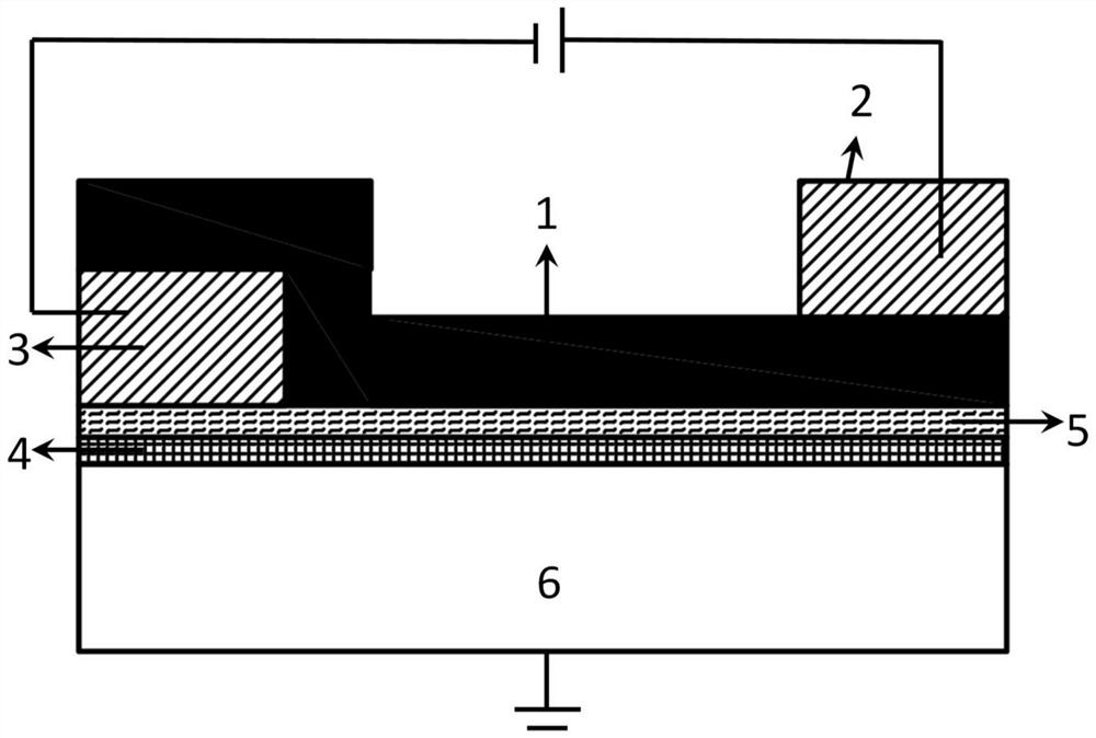
[0038] The invention provides a two-dimensional horizontal homojunction, self-driven logic photoelectric switch and its preparation method, such as figure 1 As shown, the two-dimensional horizontal homojunction in the present invention includes two-dimensional tungsten diselenide 1, gold metal p-type doping source layer 3 and indium metal n-type doping source layer 2;

[0039] The gold metal p-type doping source layer 3 is used to generate p-type doping for the two-dimensional tungsten diselenide 1;

[0040] The indium metal n-type doping source layer 2 is used to generate n-type doping to the two-dimensional tungsten diselenide 1;

[0041] The two-dimensional tungsten diselenide 1 is used as a channel and forms a p-n homojunction along the channel direction.

[0042] The gold metal p-type doping source layer 3 is arranged on one end of the two-dimensional tungsten diselenide 1, and the indium metal n-type doping source layer 2 is arranged on the two-dimensional tungsten dise...

Embodiment 1

[0057] A self-driven logic photoelectric switch, comprising two-dimensional tungsten diselenide 1, indium metal n-type doping source layer 2, gold metal p-type doping source layer 3, silicon dioxide insulating liner 4, boron nitride 5, Silicon gate electrode 6 . The gold metal p-type doping source layer 3 can generate p-type doping to the upper tungsten diselenide, and the indium metal n-type doping source layer 2 can generate n-type doping to the lower tungsten diselenide, The tungsten diselenide forms a p-n homojunction in the horizontal direction, the indium metal n-type doped source layer 2 can be used as a source and the gold metal p-type doped source layer 3 can be used as a drain to form a circuit, when two-dimensional diselenide The horizontal homojunction formed by tungsten chloride 1 can generate a voltage signal when it is illuminated, and the silicon gate electrode 6 can control the magnitude and polarity direction of the above voltage signal, so as to realize the ...

Embodiment 2

[0060] A self-driven logic photoelectric switch, comprising two-dimensional tungsten diselenide 1, indium metal n-type doping source layer 2, gold metal p-type doping source layer 3, silicon dioxide insulating liner 4, boron nitride 5, Silicon gate electrode 6 . The gold metal p-type doping source layer 3 can generate p-type doping to the upper tungsten diselenide, and the indium metal n-type doping source layer 2 can generate n-type doping to the lower tungsten diselenide, The tungsten diselenide forms a p-n homojunction in the horizontal direction, the indium metal n-type doped source layer 2 can be used as a source and the gold metal p-type doped source layer 3 can be used as a drain to form a circuit, when two-dimensional diselenide The horizontal homojunction formed by tungsten chloride 1 can generate a voltage signal when it is illuminated, and the silicon gate electrode 6 can control the magnitude and polarity direction of the above voltage signal, so as to realize the ...


PUM

PropertyMeasurementUnit
thicknessaaaaaaaaaa
thicknessaaaaaaaaaa
thicknessaaaaaaaaaa

Abstract

The invention provides a two-dimensional horizontal homojunction, self-driven logic photoelectric switch and a preparation method thereof, which belong to the field of semiconductor photoelectric technology. The photoelectric switch of the present invention comprises a two-dimensional tungsten diselenide, a silicon / silicon dioxide insulating substrate, boron nitride, an n-type doping source layer of indium metal, and a p-type doping source layer of gold metal. The invention utilizes the gold electrode to generate p-type doping to the two-dimensional tungsten diselenide, and the indium electrode to generate n-type doping to the two-dimensional tungsten diselenide, thereby constructing the two-dimensional tungsten diselenide horizontal p-n homojunction. Boron nitride and insulating silicon are used as the gate dielectric layer, and silicon is used as the gate electrode. The two-dimensional tungsten diselenide material is used as a photosensitive material to generate photo-generated electron-hole pairs under light, and a gate voltage is applied to the silicon substrate to control the rectification direction of the homojunction, thereby controlling the flow direction of photo-generated electrons and holes, and acting as a logic photoelectric switch role.

Description

【Technical field】 [0001] The invention relates to the field of semiconductor optoelectronic technology, in particular to a two-dimensional horizontal homojunction, self-driven logic photoelectric switch and a preparation method thereof. 【Background technique】 [0002] Two-dimensional homojunction and related devices have a wide range of applications in the new generation of optoelectronic devices, such as photodetection, image sensing, logic devices, memory, etc. Therefore, two-dimensional homojunction and related technologies have always been an international research hotspot and one of the main technical fields of competition in various countries. Due to their excellent carrier transport properties and strong light-matter interaction at atomic thickness, 2D materials are considered as candidate materials for next-generation novel electronic and optoelectronic devices. At present, there have been many optoelectronic devices based on two-dimensional p-n junctions, and p-n h...

Claims


Application Information

Patent Timeline
Patent Type & Authority Patents(China)
IPC IPC(8): H03K17/94H01L29/06H01L21/18
CPCH03K17/941H01L29/0603H01L29/0684H01L21/187
Inventor 张跃杜君莉张铮柳柏杉高丽于慧慧温嘉玲汤文辉张先坤洪孟雨肖建坤
Owner UNIV OF SCI & TECH BEIJING
Learn More