Optical device, optical chip loss testing device and method

A test method and technology of optical chips, which are applied in optical instrument testing, machine/structural component testing, measuring devices, etc., can solve the problems of inability to accurately calibrate the optical device under test, optical loss of optical chips, etc., so as to increase the accuracy accuracy and stability, increased flexibility, improved precision and stability

Active Publication Date: 2022-04-22
北京爱杰光电科技有限公司
View PDF0 Cites 0 Cited by
  • Summary
  • Abstract
  • Description
  • Claims
  • Application Information

AI Technical Summary

Problems solved by technology

Optical components such as optical fibers, optical couplers, and optical waveguides in test devices on the market have a certain impact on test results, and cannot accurately calibrate the optical losses of optical devices and optical chips under test. Therefore, it is urgent to invent a test with high precision. , high stability and high flexibility test device

Method used


Image

  • Optical device, optical chip loss testing device and method
  • Optical device, optical chip loss testing device and method
  • Optical device, optical chip loss testing device and method

Examples


Embodiment Construction

[0045] The following will clearly and completely describe the technical solutions in the embodiments of the present invention with reference to the accompanying drawings in the embodiments of the present invention. Obviously, the described embodiments are only some, not all, embodiments of the present invention. Based on the embodiments of the present invention, all other embodiments obtained by persons of ordinary skill in the art without making creative efforts belong to the protection scope of the present invention.

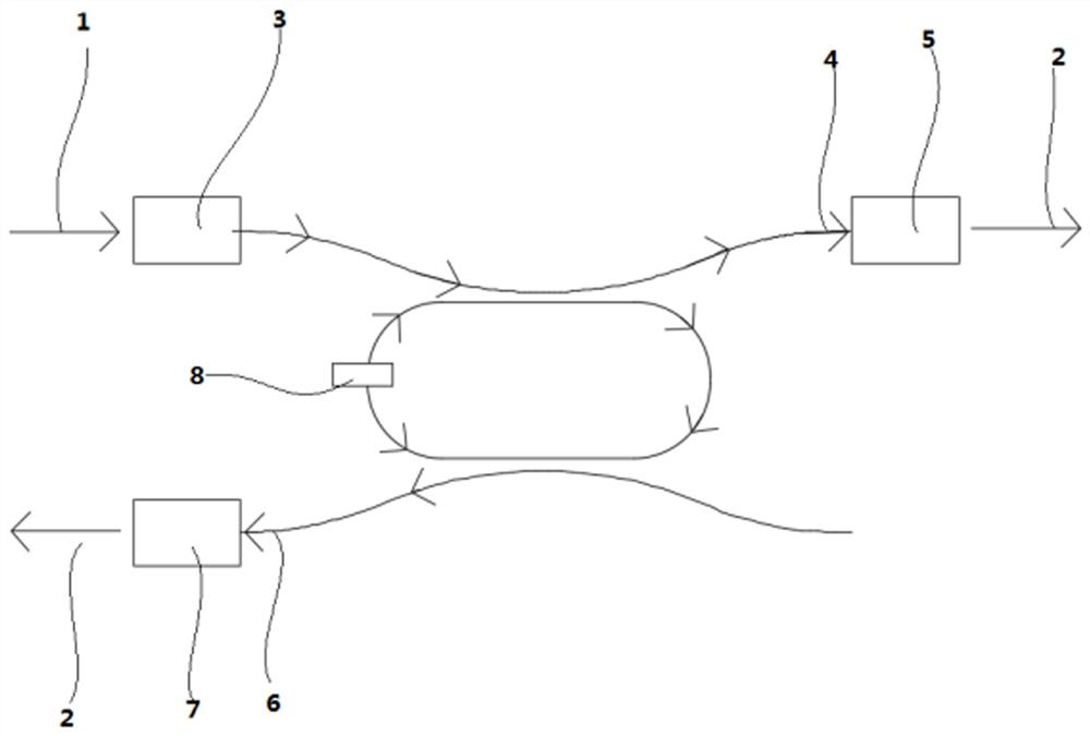
[0046] The embodiment of the present invention discloses an optical device and an optical chip loss testing device, which is characterized in that it includes a microring resonance system, an input system, and an output system;

[0047] The input system includes a first optical fiber 1 and a first optical coupler 3;

[0048] The output system includes a second optical fiber 2, a second optical coupler 5, and a third optical coupler 7;

[0049] One end of the ...


PUM


Abstract

The invention relates to the field of optical loss testing, and discloses an optical device, an optical chip loss testing device and a method, including: a micro-ring resonance system, an input system, and an output system, and the input system includes a first optical fiber and a first optical coupling device, the output system includes a second optical fiber, a second optical coupler, and a third optical coupler, one end of the first optical coupler is connected to the first optical fiber, and the other end is connected to the microring resonant system; the The second optical coupler is arranged at the upstream end of the microring resonant system, one end of which is connected to the second optical fiber, and the other end is connected to the microring resonant system; the third optical coupler is arranged at the microring resonant system The downlink end is connected with the second optical fiber at one end and connected with the micro-ring resonant system at the other end. The test accuracy, stability and flexibility are improved by embedding the optical device and optical chip under test into the micro-ring resonant system.

Description

technical field [0001] The invention relates to the field of optical loss testing, and more specifically relates to an optical device and an optical chip loss testing device and method. Background technique [0002] Optical loss is an important parameter index to measure the performance of optical devices and optical chips, and determines the application scenarios of optical devices and optical chips. Typical optical test setups require perfect alignment of the fiber and optical coupler, requiring the fiber to be at the same physical location for each test. Optical components such as optical fibers, optical couplers, and optical waveguides in test devices on the market have a certain impact on test results, and cannot accurately calibrate the optical loss of the optical device and optical chip under test. Therefore, it is urgent to invent a test with high precision. , high stability and high flexibility test device. Contents of the invention [0003] In view of this, the...

Claims


Application Information

Patent Timeline
Patent Type & Authority Patents(China)
IPC IPC(8): G01M11/02
CPCG01M11/0292
Inventor 周治平杨丰赫
Owner 北京爱杰光电科技有限公司
Why Eureka
Try Eureka