Printed circuit board surface defect positioning and identifying method

A printed circuit board and identification method technology, which is applied in image data processing, image enhancement, instruments, etc., can solve the problems of detection accuracy and detection speed that need to be further improved

Active Publication Date: 2020-06-09
HUNAN UNIV
View PDF12 Cites 10 Cited by
  • Summary
  • Abstract
  • Description
  • Claims
  • Application Information

AI Technical Summary

Problems solved by technology

However, due to the influence of lighting conditions, industrial site environment and other factors, the original images collected by ind

Method used


Image

  • Printed circuit board surface defect positioning and identifying method
  • Printed circuit board surface defect positioning and identifying method
  • Printed circuit board surface defect positioning and identifying method

Examples


Embodiment Construction

[0062] It should be noted that, in the case of no conflict, the embodiments of the present invention and the features in the embodiments can be combined with each other. The present invention will be described in detail below with reference to the accompanying drawings and examples.

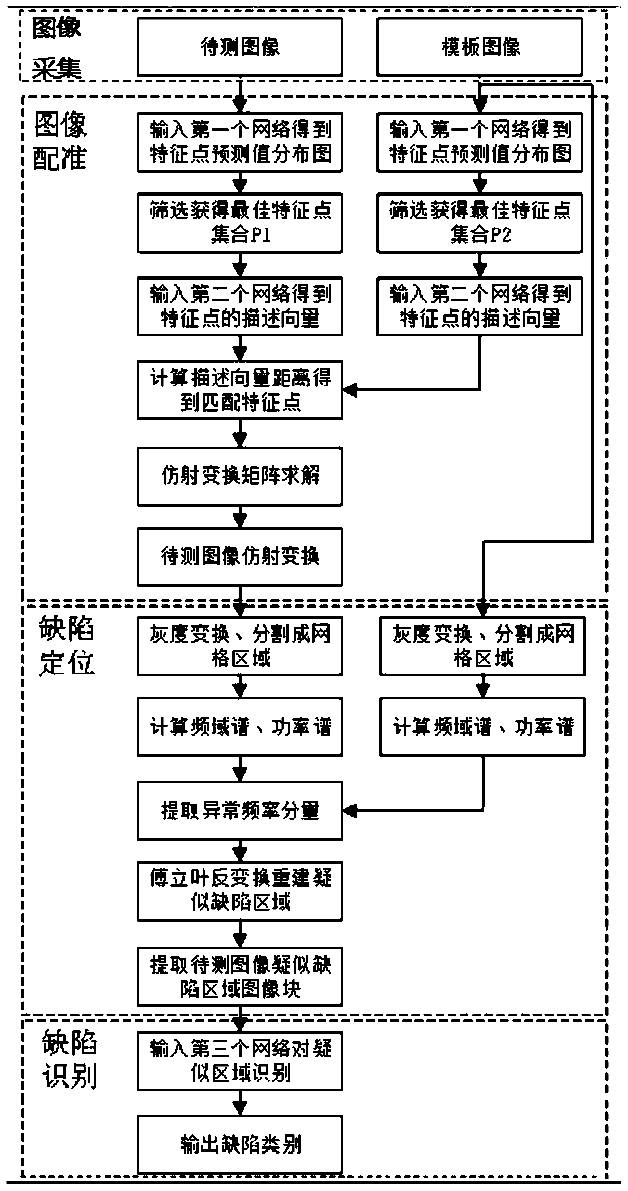
[0063] figure 1 It is a flow chart of a method for locating and identifying surface defects of a printed circuit board according to an embodiment of the present invention. Such as figure 1 As shown, the method sequentially includes four processes of image acquisition, image registration, defect location and defect recognition, specifically:

[0064] (1) Image collection, collecting the image I(x,y) of the printed circuit board to be tested and the image T(x,y) of the template;

[0065] (2) Image registration, accurately register the image to be tested I(x,y) and the template image T(x,y) through two convolutional neural networks, and obtain the image to be tested after registration Preferabl...


PUM


Abstract

The invention discloses a printed circuit board surface defect positioning and identification method. The method comprises the following steps: firstly, collecting a to-be-detected image and a template image of a printed circuit board; secondly, using a first convolutional neural network to obtain a feature point prediction distribution map, and screening to obtain an optimal feature point; then,calculating a description vector of the optimal feature point by using a second convolutional neural network, and matching the optimal feature points of the to-be-detected image and the template image; then, calculating an affine transformation matrix according to the matching points, and projecting the image to be measured onto the template image; thirdly, calculating a power spectrum of the projected to-be-detected image and the template image, obtaining an abnormal frequency component of the to-be-detected image according to the power spectrum difference, and obtaining a suspected defect area through inverse Fourier transform; and finally, identifying and classifying the suspected defect area by using a third convolutional neural network. According to the method, the surface defects ofthe printed circuit board can be accurately positioned and identified, the quality of the circuit board is guaranteed, and the method has certain robustness to environmental noise.

Description

technical field [0001] The invention relates to the technical field of machine vision and pattern recognition detection, in particular to a method for locating and identifying defects on the surface of a printed circuit board. Background technique [0002] Printed circuit board (PCB), as a carrier for electrical connection and fixing of electronic components, has been widely used in many fields of modern production and manufacturing. The quality of modern electronic equipment depends not only on the quality and performance of electronic components, but also largely on the quality of printed circuit boards. The development trend of integration and miniaturization of electronic components makes the manufacturing process of PCB more and more complicated. Due to factors such as equipment, environment and human error, there will be defects such as short circuits, open circuits, scratches and holes in PCB production that affect product performance. . [0003] Traditional human e...

Claims


Application Information

Patent Timeline
IPC IPC(8): G06T7/00G06T7/30G06N3/04
CPCG06T7/0014G06T7/30G06T2207/30148G06N3/045Y02P90/30
Inventor 袁小芳谢黎刘琛王耀南
Owner HUNAN UNIV
Why Eureka
Try Eureka