
Eureka
For R&D, Eureka makes reading and utilizing patents & technical documents easy.
Eureka AIR
Designed for self-driven R&D workflows. Generate viable solutions, solve complex R&D challenges, empower your innovation with AI.

Eureka Materials
Designed for material experts only. Revolutionize your material R&D, from search, analyze, to developing new materials.

TechResearch
Generate reliable direction feasibility study reports for your R&D in just a few steps.

TechSeek
Discover and master advanced knowledge NOW. Basics, ideas, possibilities, all at once.

TechMind
As an expert in R&D Theories, TechMind can generates customized viable solutions instantly.

TechRisk
Analyze your overall solution with one click, know your potential R&D risks in advance.

TechMonitor
Get weekly tech updates, stay abreast of the latest tech innovations and key insights.
Design product structure and method for manufacturing 5G circuit board
A circuit board manufacturing and design method technology, applied in multilayer circuit manufacturing, printed circuit manufacturing, printed circuit, etc., can solve problems such as pressing bonding force and lack of signal conductivity of finished products
- Summary
- Abstract
- Description
- Claims
- Application Information
AI Technical Summary
Problems solved by technology
Method used
Image


Examples
Embodiment Construction
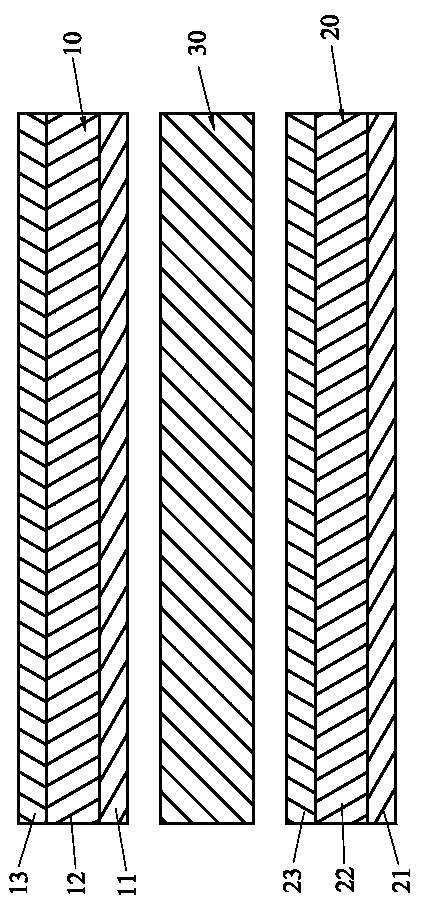
[0026] The present invention discloses a design product structure for 5G circuit board manufacturing, such as image 3 As shown, it includes an upper core board 10 , a lower core board 20 and a connection curing sheet 30 .
[0027] The upper core board 10 includes a first lower copper foil layer 11, a first cured sheet 12, and a first upper copper foil layer 13 that are laminated and fixed together from bottom to top; the lower core board 20 includes a bottom-up The second lower copper foil layer 21, the second cured sheet 22, and the second upper copper foil layer 23 are stacked and fixed together; the connected cured sheet 30 is sandwiched between the upper core board 10 and the lower core board 20, and the second Both the lower copper foil layer 11 and the second upper copper foil layer 23 are reversed copper foils, and are attached and fixed to the upper and lower surfaces of the connection curing sheet 30 respectively.
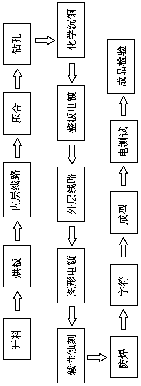
[0028] Such as figure 1 As shown, the present inv...
PUM
 Abstract
Description
Claims
Application Information
 - R&D Engineer
- R&D Manager
- IP Professional
- Industry Leading Data Capabilities
- Powerful AI technology
- Patent DNA Extraction
Browse by: Latest US Patents, China's latest patents, Technical Efficacy Thesaurus, Application Domain, Technology Topic, Popular Technical Reports.
© 2024 PatSnap. All rights reserved.Legal|Privacy policy|Modern Slavery Act Transparency Statement|Sitemap|About US| Contact US: help@patsnap.com