
Optical coating element surface shape compensation method based on mixture single-layer film

A compensation method and single-layer film technology, applied in coating, sputtering coating, vacuum evaporation coating and other directions, can solve the problems of increasing coating cost and difficult preparation process, and achieve the effect of reducing the quality of wavefront

Active Publication Date: 2020-06-16
SHANGHAI INST OF OPTICS & FINE MECHANICS CHINESE ACAD OF SCI
View PDF7 Cites 2 Cited by
  • Summary
  • Abstract
  • Description
  • Claims
  • Application Information

AI Technical Summary

Problems solved by technology

[0004] One is to coat a silicon dioxide film layer on the non-coated surface of the substrate to offset the stress on the functional film surface. This compensation technology is only applicable to substrates with a refractive index close to that of silicon dioxide materials, such as fused silica substrates;
[0005] The second is to coat the same film layer on both sides of the substrate. This method increases the coating cost and is not suitable for thin-film components that require different technical indicators on both sides of the substrate;
[0006] The third is to use different deposition techniques to prepare high and low refractive index layers, such as the use of atomic layer deposition technology to prepare Al 2 o 3 , prepared SiO by ion beam sputtering 2 layer (see Applied Surface Science, 2019, 476:521-527), this method needs to replace the coating equipment every time a layer of film is prepared, and the actual preparation process is extremely difficult

Method used


Image

  • Optical coating element surface shape compensation method based on mixture single-layer film
  • Optical coating element surface shape compensation method based on mixture single-layer film
  • Optical coating element surface shape compensation method based on mixture single-layer film

Examples


Embodiment Construction

[0031] The present invention will be further described below in conjunction with the embodiments and accompanying drawings.

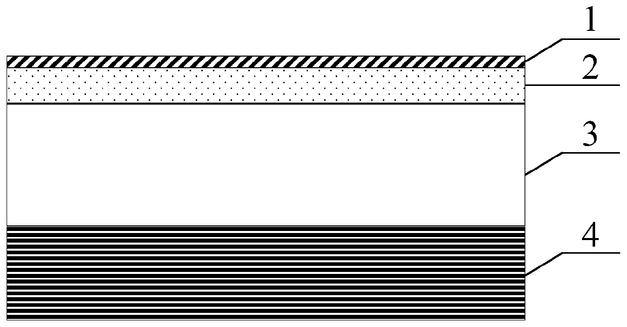
[0032] see first figure 1 , figure 1 It is a schematic diagram of a physical embodiment of the surface shape compensation of an optical coating element based on a mixture monolayer film of the present invention.

[0033] With K9 glass as the substrate, using HfO 2 and SiO 2 As the high and low refractive index materials in the mixture single-layer film, the surface compensation of the single-sided 1064nm high-reflection film is taken as an example, and the method for compensating the surface shape of the optical coating element based on the mixture single-layer film of the present invention is described. The method includes the following steps :

[0034] ① Input parameters to the computer: including the substrate refractive index n S (1.51), the refractive index n of ion beam-assisted deposition of high refractive index materials H (1.90), the ref...


PUM


Abstract

The invention discloses an optical coating element surface shape compensation method based on a mixture single-layer film. An ion beam auxiliary mixture single-layer film is deposited on a non-coatingsurface of a substrate or a surface to be coated with a concave surface shape after coating by using an electron beam double-source co-evaporation technology and an ion beam auxiliary deposition technology at the same time, and an optical dummy layer with the same refractive index as the substrate is formed to tune the surface shape of a coating element. According to the method, surface shape compensation can be carried out on the coating element deposited on the substrate with any refractive index, the quality reduction of the wave surface caused by coating is reduced, the spectral performance of the coating element is not influenced, and the method is suitable for single-sided coating elements and double-sided coating elements.

Description

technical field [0001] The invention relates to an optical thin film, in particular to a method for compensating the surface shape of an optical coating element based on a mixture monolayer film. Background technique [0002] Wavefront quality is one of the performance parameters of optical thin-film components, and the wavefront quality of thin-film components will affect the beam output quality of laser devices. The intrinsic stress of the film layer will cause the wavefront quality of the coated component to change after coating, and the surface shape compensation technology is an effective technical way to improve the wavefront quality of the coated component. The surface shape compensation technology currently used includes substrate pre-surface shape technology and film layer stress compensation technology. The substrate pre-surface shape technology processes the substrate into the opposite surface shape according to the surface shape change caused by the film layer. ...

Claims


Application Information

Patent Timeline
Patent Type & Authority Applications(China)
IPC IPC(8): C23C14/30C23C14/46C23C14/10C23C14/08
CPCC23C14/083C23C14/10C23C14/30C23C14/46
Inventor 朱美萍李静平邵建达赵娇玲宋晨郭猛刘晓凤王胭脂
Owner SHANGHAI INST OF OPTICS & FINE MECHANICS CHINESE ACAD OF SCI
Learn More