Supercharge Your Innovation With Domain-Expert AI Agents!

Display panel and display device

A technology for display panels and substrates, applied in electrical components, electrical solid devices, circuits, etc., can solve the problems of uneven evaporation, affecting product quality, uneven Pixel light emission, etc., to improve utilization efficiency, improve brightness uniformity, The effect of increasing the brightness of the light

Inactive Publication Date: 2020-06-16
WUHAN CHINA STAR OPTOELECTRONICS SEMICON DISPLAY TECH CO LTD
View PDF3 Cites 1 Cited by
  • Summary
  • Abstract
  • Description
  • Claims
  • Application Information

AI Technical Summary

Problems solved by technology

[0003] Different from LCD, AMOLED adopts an active light-emitting method, and each pixel (Pixel) unit emits light independently; therefore, it is very easy to have the problem of uneven light emission of Pixels in different areas of the panel
For example, factors such as uneven evaporation and different decay speeds of OLEDs of different colors will lead to uneven light emission of Pixels in different areas of the panel, resulting in uneven display of the entire panel and seriously affecting product quality.

Method used


Image

  • Display panel and display device
  • Display panel and display device
  • Display panel and display device

Examples


Embodiment Construction

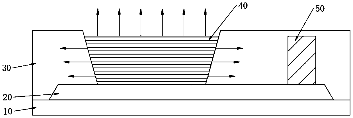
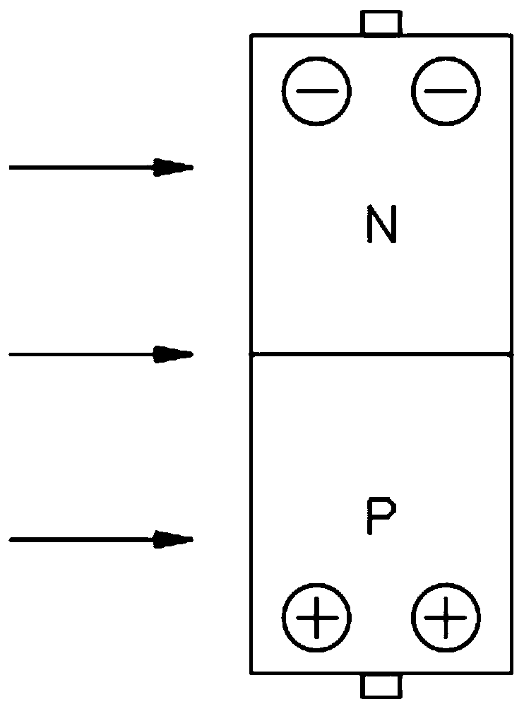
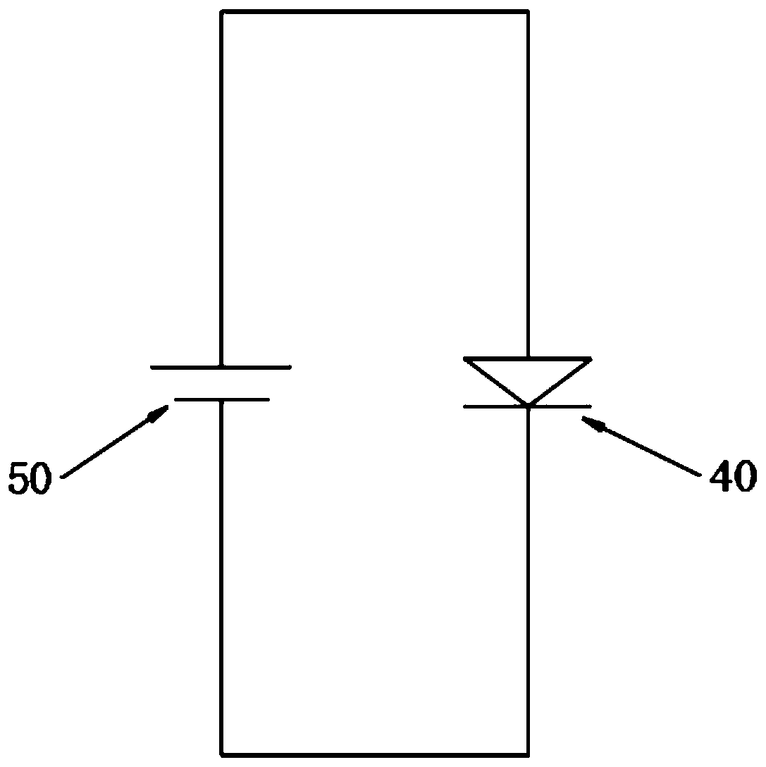
[0024] The following will clearly and completely describe the technical solutions in the embodiments of the present invention with reference to the drawings in the embodiments of the present invention. Apparently, the described embodiments are only some of the embodiments of the present invention, but not all of them. Based on the embodiments of the present invention, all other embodiments obtained by those skilled in the art without creative efforts fall within the protection scope of the present invention.

[0025] In describing the present invention, it should be understood that the terms "center", "longitudinal", "transverse", "length", "width", "thickness", "upper", "lower", "front", " Orientation indicated by rear, left, right, vertical, horizontal, top, bottom, inside, outside, clockwise, counterclockwise, etc. The positional relationship is based on the orientation or positional relationship shown in the drawings, which is only for the convenience of describing the pr...


PUM


Abstract

The embodiment of the invention discloses a display panel and a display device. The display panel comprises a substrate, an anode layer, a pixel defining layer and an OLED device, wherein the anode layer is arranged on the substrate; the pixel defining layer is arranged on the anode layer and the substrate; the OLED device is arranged in the pixel defining layer; and a photoelectric converter is further arranged in the pixel defining layer, and the photoelectric converter is arranged on the anode layer and is adjacent to the OLED device. According to the embodiment of the invention, the photoelectric converter is arranged in the pixel defining layer, so that light of the OLED device can be absorbed and converted into electric energy, and the electric energy can be directly used for compensating the OLED device with relatively low brightness and relatively fast attenuation on the one hand; and on the other hand, the brightness of the corresponding pixel unit is judged by monitoring theelectric signal, so that the OLED device with relatively low brightness and relatively fast attenuation is compensated through a pixel driving circuit, and the overall brightness uniformity of the panel can be improved in two aspects.

Description

technical field [0001] The present invention relates to the field of display technology, in particular to a display panel and a display device. Background technique [0002] Active-matrix organic light emitting diode panel (Active-matrix organic light emitting diode, AMOLED) has self-illuminating characteristics, using flexible substrates, flexible low-temperature polysilicon technology (LowTemperature Poly-silicon, LTPS) process and high-efficiency organic light-emitting diodes ( Organic Light-Emitting Diode, OLED) display technology. Compared with Liquid Crystal Display (LCD), AMOLED panel is self-illuminating, does not require backlight, has fast response, high color gamut, high contrast, wide viewing angle, wide viewing angle, low power consumption, foldable, and light weight , thin thickness, simple structure, low cost and other advantages, it is regarded as one of the most promising products. [0003] Unlike liquid crystals, AMOLED uses an active light emitting metho...

Claims


Application Information

Patent Timeline
IPC IPC(8): H01L27/32
CPCH10K59/60H10K59/122H10K59/12
Inventor 郭庆勋王硕晟
Owner WUHAN CHINA STAR OPTOELECTRONICS SEMICON DISPLAY TECH CO LTD
Features
  • R&D
  • Intellectual Property
  • Life Sciences
  • Materials
  • Tech Scout
  • Unparalleled Data Quality
  • Higher Quality Content
  • 60% Fewer Hallucinations
Learn More