Circuit board welding forming method

A welding forming and circuit board technology, which is applied in welding equipment, auxiliary devices, metal processing, etc., can solve the problems of poor subsequent processing of circuit boards, affecting the use of circuit boards, affecting the safety of circuit boards, etc., to achieve shearing effect Good, avoid bending, prevent cross-short circuit effect

Active Publication Date: 2020-06-19
GUANGZHOU HONGYU SCI & TECH
View PDF6 Cites 1 Cited by
  • Summary
  • Abstract
  • Description
  • Claims
  • Application Information

AI Technical Summary

Problems solved by technology

[0005] The present invention can solve the problem that the existing equipment cannot accurately position the circuit board when welding the circuit board, resulting in poor subsequent processing effect of the circuit board and affecting the use effect of the circuit board. When the pins of the circuit board are cut, the cutting effect is poor, the cutting is incomplete, and the pins are prone to bending during cutting, which leads to the phenomenon that the pins of the electrical components are prone to cross-short circuit when the circuit board is installed and used later. , affecting the safety of circuit board use and other problems

Method used


Image

  • Circuit board welding forming method
  • Circuit board welding forming method
  • Circuit board welding forming method

Examples


Embodiment Construction

[0036] The embodiments of the present invention will be described in detail below with reference to the accompanying drawings, but the present invention can be implemented in many different ways defined and covered by the claims.

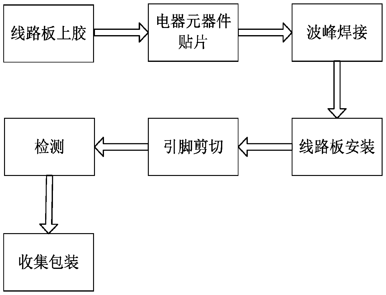
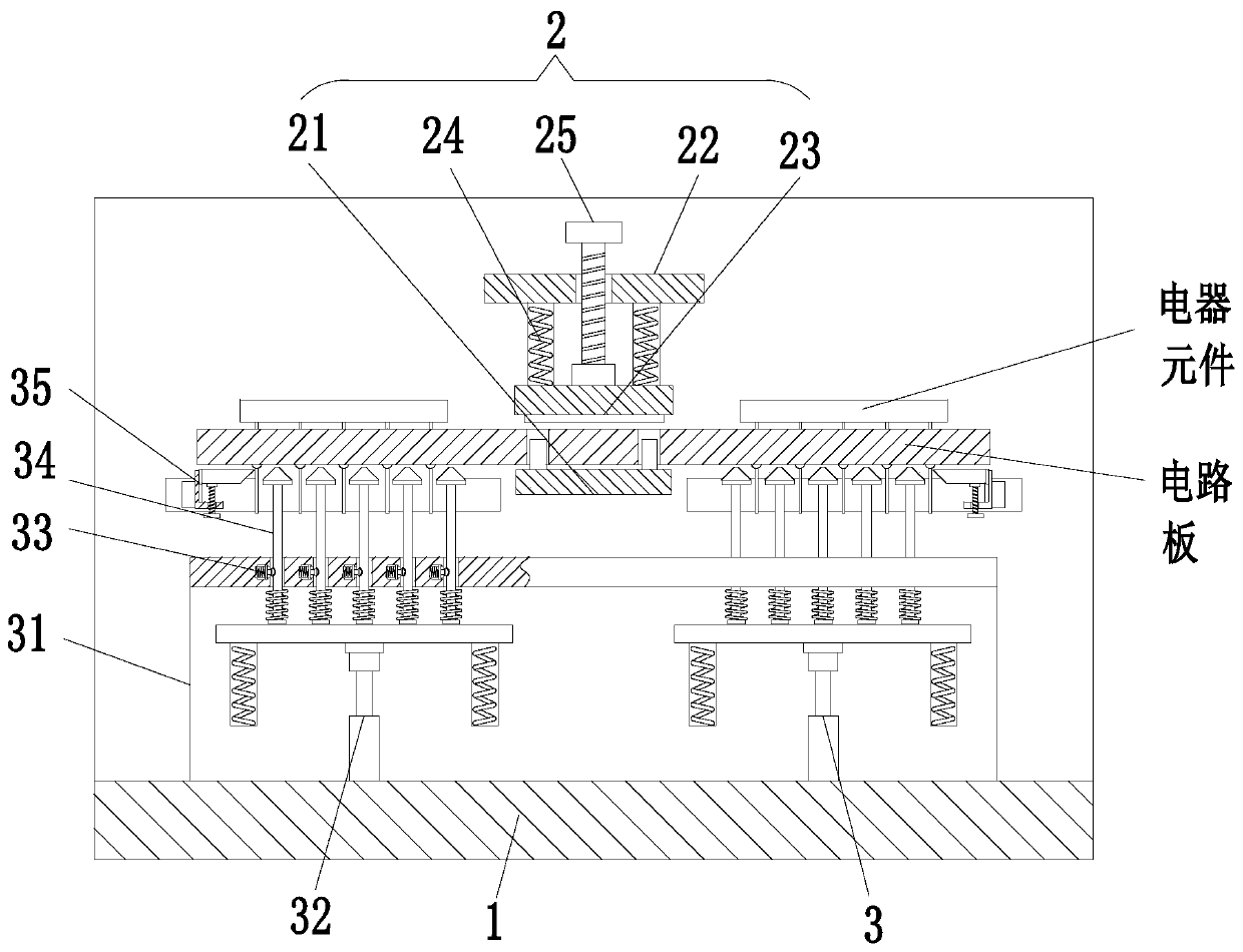
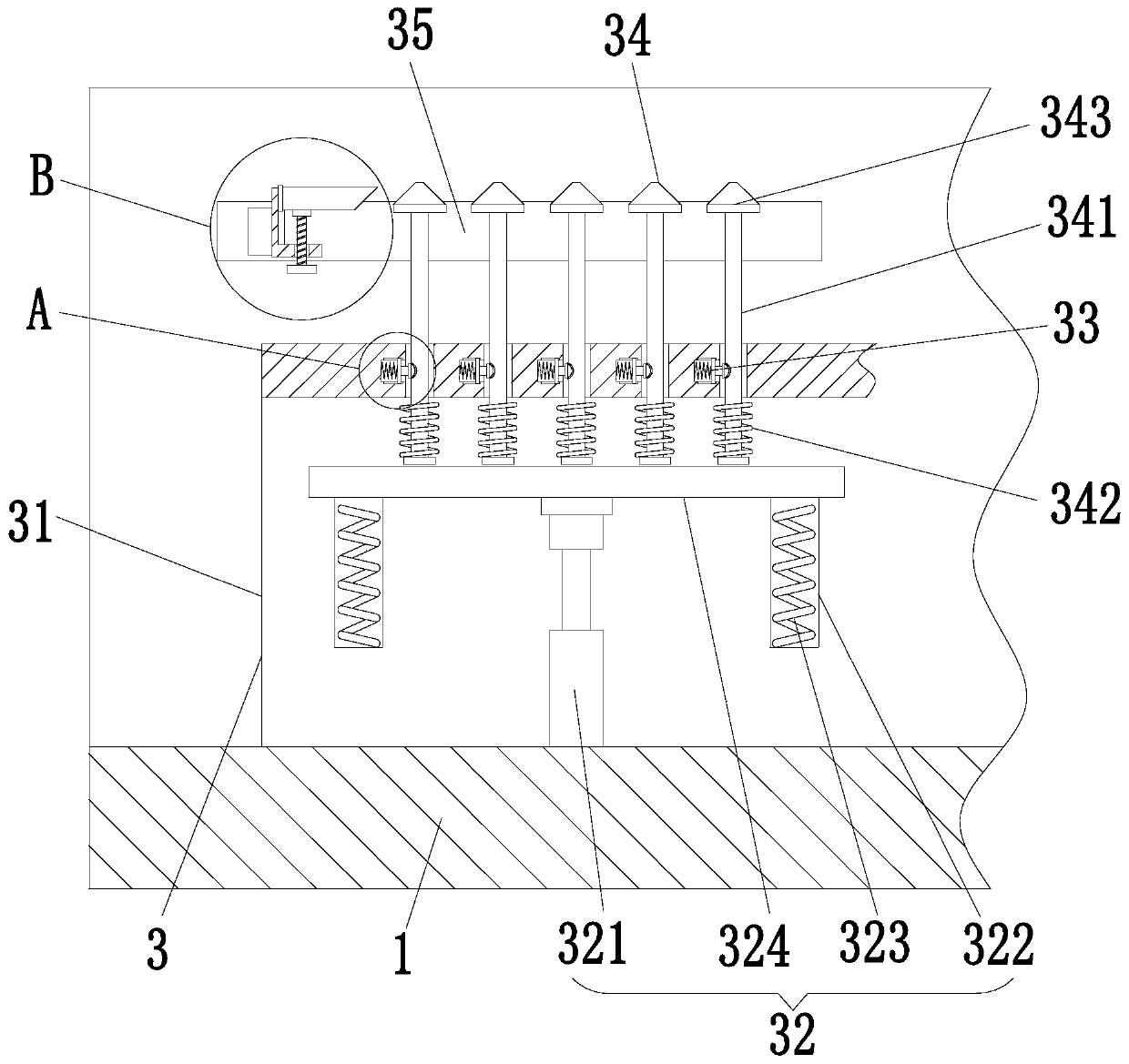
[0037] Such as Figure 1 to Figure 7 Shown, a kind of circuit board soldering forming method comprises the following steps:

[0038] S1. Glue on the circuit board: Manually apply a layer of adhesive on the position of the electrical components to be welded on the circuit board, and the adhesive is applied evenly, and the area of ​​the application is smaller than the area of ​​the electrical components;

[0039] S2. Electrical component patch: pass the electrical component pins to be soldered through the through holes on the circuit board manually, and the electrical components are bonded with the adhesive, and the adhesive applied in step S1 is glued with an oven or tunnel furnace curing;

[0040] S3. Wave soldering: use wave soldering to connect ...


PUM


Abstract

The invention relates to a circuit board welding forming method. A fixing frame, a clamping device and shearing devices are included; the fixing frame is of a U-shaped structure; the clamping device is fixedly installed in the middle of the interior of the fixing frame; the shearing devices are symmetrically arranged on the outer side of the clamping device; and the shearing devices are installedat the lower end of the interior of the fixing frame. By means of the method, the problems that existing equipment cannot accurately position a circuit board when carrying out welding processing on the circuit board, consequently, the subsequent processing effect of the circuit board is poor and the use effect of the circuit board is influenced, besides, when pins of the circuit board are cut by the existing equipment, the cutting effect is poor, cutting is incomplete, the pins are prone to bending when cut, consequently, pins of electrical components are prone to cross short circuit when thecircuit board is installed and used later, and the use safety of the circuit board is affected can be solved.

Description

technical field [0001] The invention relates to the technical field of circuit board welding processing, in particular to a circuit board welding forming method. Background technique [0002] The circuit board can be called a printed circuit board or a printed circuit board. The circuit board makes the circuit miniaturized and intuitive, and plays an important role in the mass production of fixed circuits and the optimization of the layout of electrical appliances. The support body is also the carrier for the electrical connection of electronic components. [0003] At present, the existing circuit boards usually have the following defects when welding the circuit boards: 1. The existing equipment cannot accurately position the circuit boards when welding the circuit boards, resulting in the subsequent processing of the circuit boards. 2. When the existing equipment cuts the pins of the circuit board, the cutting effect is poor and the cutting is incomplete. The pins are pro...

Claims


Application Information

Patent Timeline
Patent Type & Authority Applications(China)
IPC IPC(8): B23K3/00B23K3/08
CPCB23K3/00B23K3/08
Inventor 王强顾小东
Owner GUANGZHOU HONGYU SCI & TECH
Why Eureka
Try Eureka