Online detection method and system for PCB production process of intelligent production line

A technology of production process and detection method, applied in the direction of neural learning method, measuring device, CAD circuit design, etc., can solve the problems of incompleteness and single detection, and achieve the effect of improving yield rate, accuracy and lighting uniformity

Active Publication Date: 2020-06-19
湖南珞佳智能科技有限公司
View PDF7 Cites 3 Cited by
  • Summary
  • Abstract
  • Description
  • Claims
  • Application Information

AI Technical Summary

Problems solved by technology

[0003] The purpose of the present invention is to overcome the single and incomplete problem of defect detection in the PCB manufacturing process in the prior art

Method used


Image

  • Online detection method and system for PCB production process of intelligent production line
  • Online detection method and system for PCB production process of intelligent production line
  • Online detection method and system for PCB production process of intelligent production line

Examples


Embodiment Construction

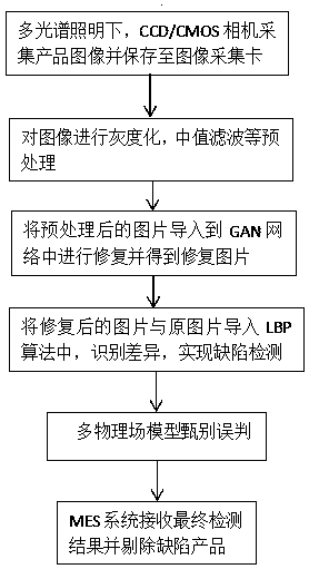
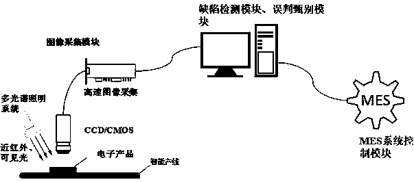
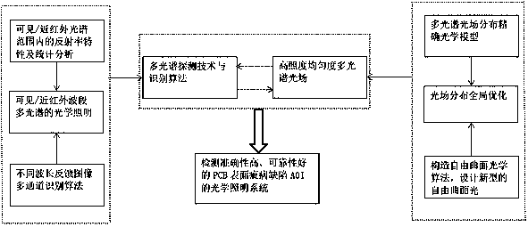
[0033] The following will clearly and completely describe the technical solutions in the embodiments of the present invention with reference to the accompanying drawings in the embodiments of the present invention. Obviously, the described embodiments are only some, not all, embodiments of the present invention. Based on the embodiments of the present invention, all other embodiments obtained by persons of ordinary skill in the art without making creative efforts belong to the protection scope of the present invention.

[0034] In describing the present invention, it is to be understood that the terms "center", "upper", "lower", "front", "rear", "left", "right", "vertical", "horizontal", The orientations or positional relationships indicated by "top", "bottom", "inner", "outer", etc. are based on the orientations or positional relationships shown in the drawings, and are only for the convenience of describing the present invention and simplifying the description, rather than in...


PUM


Abstract

The invention belongs to the technical field of additive manufacturing, and particularly provides an online detection method and system for a PCB production process of an intelligent production line,and the method comprises the steps: S1, collecting a surface image of an electronic device on the intelligent production line in a multispectral illumination environment; s2, performing defect detection on the surface image; s3, misjudging and discriminating a defect detection result; and S4, importing a final detection result after misjudgment and discrimination into the intelligent production line for feedback regulation. The surface illumination uniformity of the tested electronic product is remarkably improved through the multispectral illumination environment, and then the image recognition accuracy is improved; defect detection is carried out by using a deep network, and misjudgment and discrimination are carried out by using a multi-physical-field model, so that a more reliable detection result is obtained. Finally, the product is repaired or removed according to the detection result, damage is stopped in time, and the yield is increased.

Description

technical field [0001] The invention belongs to the technical field of machine vision detection, and in particular relates to an online detection method and system for the PCB production process of an intelligent production line. Background technique [0002] Printed circuit board PCB (printed circuit board), referred to as printed board, is one of the important components of the electronics industry. Printed boards are used in almost every electronic device that has electronic components such as integrated circuits. However, due to the complex manufacturing environment of more and more PCBs and the large number of process steps, there are more and more defects (such as warping, delamination, cracks, short circuits, etc.). Therefore, the importance of defect detection in the printed circuit board manufacturing process is also increasing. Therefore, the importance of defect detection in the printed circuit board manufacturing process is also increasing. At present, manual ...

Claims


Application Information

Patent Timeline
Patent Type & Authority Applications(China)
IPC IPC(8): G01N21/88G01N21/956G06T7/00G06T5/00G06F30/39G06F30/23G06N3/08
CPCG01N21/8806G01N21/8851G01N21/956G01N21/95607G01N2021/8887G01N2021/95638G06N3/08G06T5/002G06T7/0004G06T2207/20032
Inventor 刘胜李辉王浩丞黄贻苍韩金哲
Owner 湖南珞佳智能科技有限公司
Why Eureka
Try Eureka