Automatic visual inspection system of PCB and working method of automatic visual inspection system
A PCB circuit board, visual inspection technology, applied in measurement devices, optical testing of flaws/defects, material analysis by optical means, etc., can solve problems such as size error, component shape error, low efficiency, etc. The effect of efficiency
- Summary
- Abstract
- Description
- Claims
- Application Information
AI Technical Summary
Problems solved by technology
Method used
Image
Examples
Embodiment Construction
[0041] The present invention will be further described below in conjunction with the accompanying drawings.
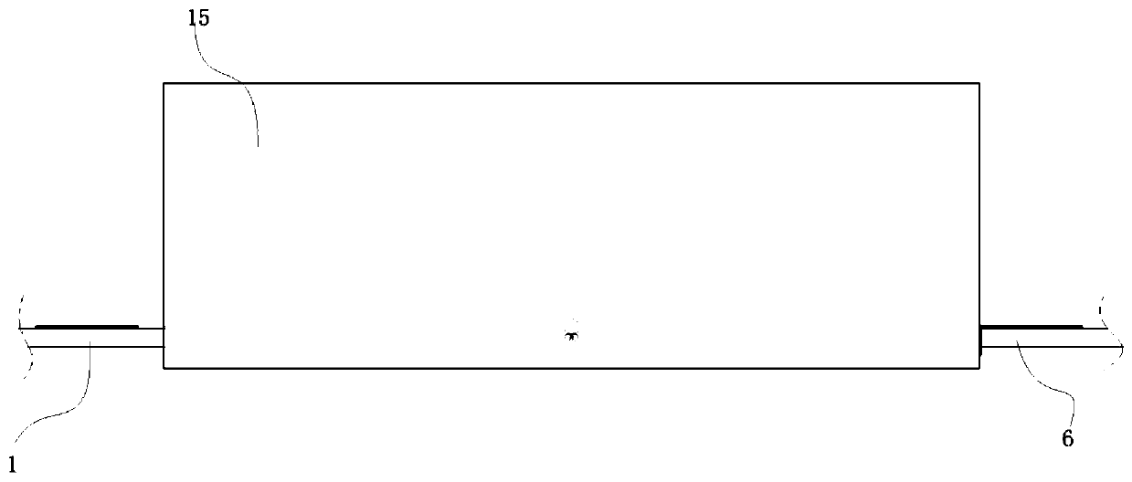
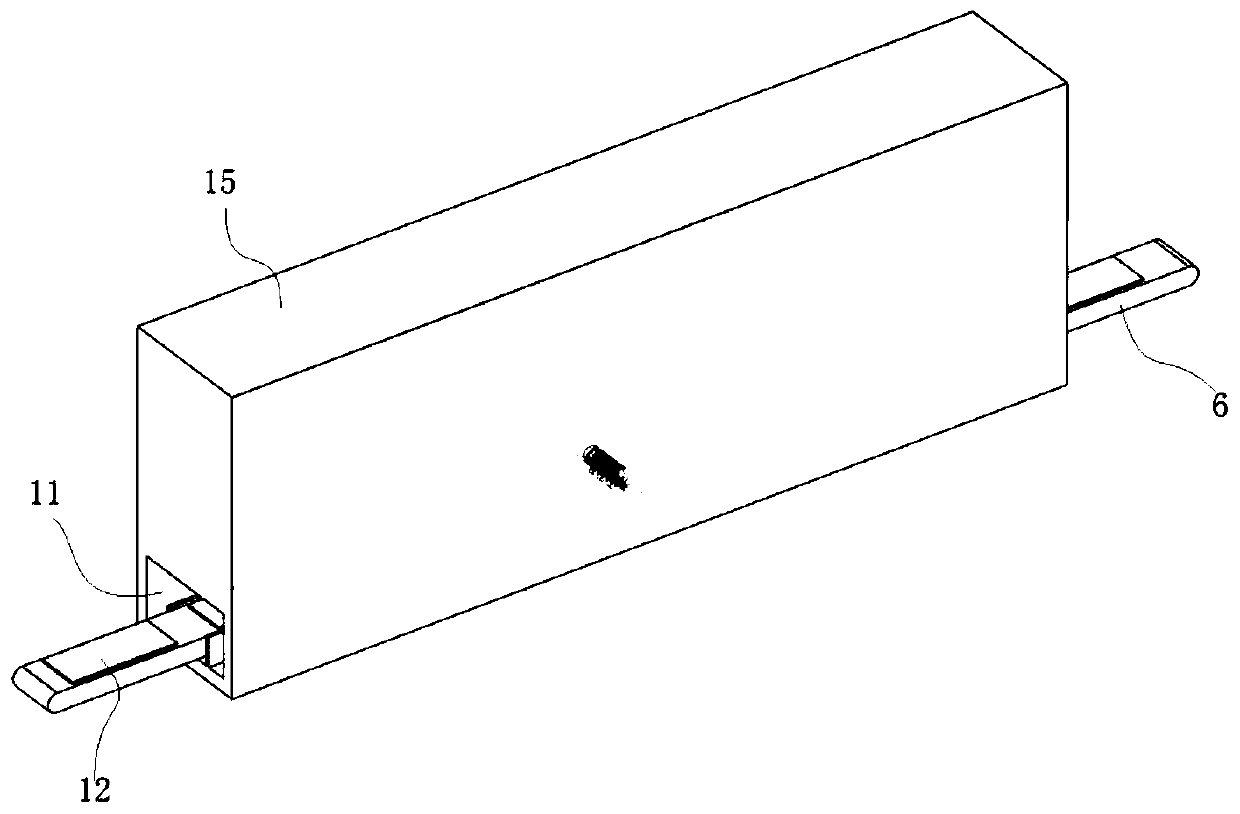
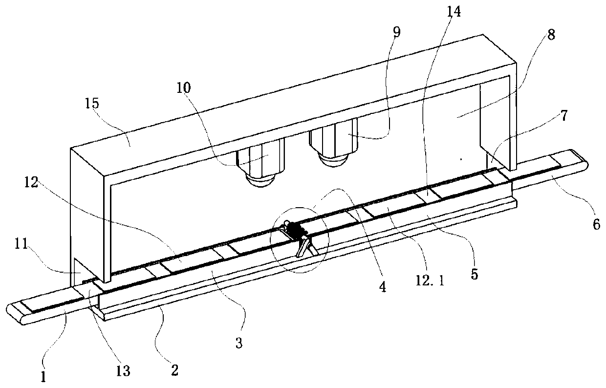
[0042] as attached Figures 1 to 12 The automatic visual detection system of the PCB circuit board shown includes a dark box 15, and the inside of the dark box 15 is a visual inspection room 8, and an industrial camera is arranged inside the visual inspection room 8;
[0043] The lower side of the front and rear walls of the dark box 15 are respectively provided with a front transfer port 11 and a rear transfer port 7 that pass through the inside of the visual inspection chamber 8; The conveying surface 13 is flat with the rear conveying surface 14 on the rear conveyor belt unit 6; both the front conveying surface 13 and the rear conveying surface 14 can horizontally convey the PCB board along the length direction;
[0044] The outgoing end of the front conveyor belt unit 1 passes through the front transmission port 11 along the front-rear direction and extends horizo...
PUM
 Abstract
Description
Claims
Application Information


