OLED display panel and manufacturing method thereof, and display device

A display panel and display area technology, which is applied in the field of OLED, can solve problems such as low product yield and affecting the display quality of product display areas, and achieve the effect of eliminating gaps

Active Publication Date: 2020-07-03
EVERDISPLAY OPTRONICS (SHANGHAI) CO LTD
View PDF4 Cites 0 Cited by
  • Summary
  • Abstract
  • Description
  • Claims
  • Application Information

AI Technical Summary

Problems solved by technology

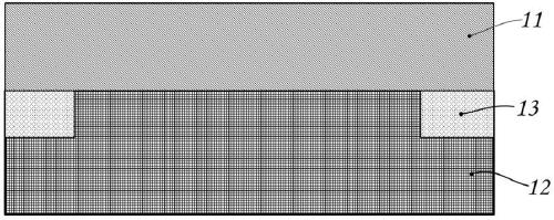
[0004] like figure 1 As shown, the lower part of the existing cover plate 11 is provided with a shielding layer 13. Due to the existence of the shielding layer 13, the bonding surface located in the display area of ​​the cover plate 11 and the shielding layer located in the peripheral area of ​​the cover plate 11 13, there is a difference in height between the bonding surface of the cover plate 11, so that an ink step or a gap is formed at the junction of the display area of ​​the cover plate 11 and the peripheral area of ​​the cover plate 11, which in turn causes the optical The adhesive layer 12 cannot fully fill the step gap at the junction of the bonding surface of the display area of ​​the cover plate 11 and the bonding surface of the peripheral area of ​​the cover plate 11, forming bonding bubbles in the display area of ​​the cover plate 11, affecting the quality of the display area of ​​the product. Display quality, thus making the product yield lower

Method used


Image

  • OLED display panel and manufacturing method thereof, and display device
  • OLED display panel and manufacturing method thereof, and display device
  • OLED display panel and manufacturing method thereof, and display device

Examples


Embodiment Construction

[0059] The following will clearly and completely describe the technical solutions in the embodiments of the present invention with reference to the accompanying drawings in the embodiments of the present invention. Obviously, the described embodiments are only some, not all, embodiments of the present invention. Based on the embodiments of the present invention, all other embodiments obtained by persons of ordinary skill in the art without creative efforts fall within the protection scope of the present invention.

[0060] "First", "second" and similar words used in the present disclosure do not indicate any order, quantity or importance, but are only used to distinguish different components. "Comprising" or "comprising" and similar words mean that the elements or items appearing before the word include the elements or items listed after the word and their equivalents, without excluding other elements or items. Words such as "connected" or "connected" are not limited to physic...


PUM


Abstract

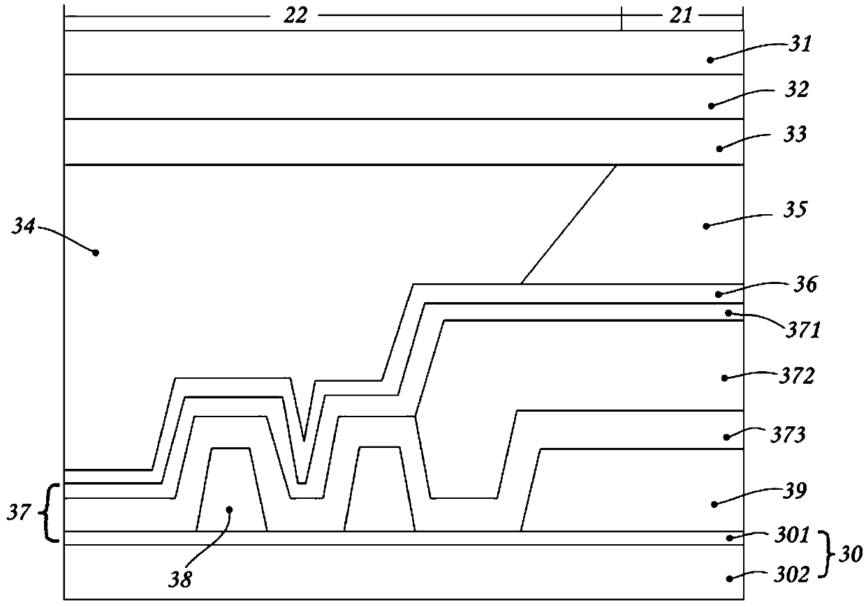
The invention discloses an OLED display panel and a manufacturing method thereof, and a display device. The OLED display panel comprises an array substrate, a pixel light-emitting layer, a touch control layer, a planarization layer and a cover plate which are sequentially arranged in a stacked mode, and further comprises a first shielding layer is formed between the touch control layer and the cover plate and located on the same layer as the planarization layer, wherein the planarization layer is formed in a display area, and the first shielding layer is formed in the peripheral area surrounding the planarization layer. According to the invention, the first shielding layer is arranged between the polarization layer and the touch control layer, so that no step offset exists between the first shielding layer and the planarization layer so as to eliminate the offset of the shielding layer and effectively shield the non-display circuit at the bottom; and through the second shielding layerarranged between the touch control layer and the packaging layer, the bottom non-display circuit can be further shielded, and the touch layer can be free of bending, so that the circuit in the touch layer is prevented from being broken, and the flexibility of the touch layer is improved.

Description

technical field [0001] The present invention relates to a technology in the OLED field, and more specifically, relates to an OLED display panel, a manufacturing method thereof and a display device. Background technique [0002] With the development of science and technology, more and more electronic products appear in people's lives, from small products such as mobile phones, personal digital assistants (Personal Digital Assistant, PDA), digital cameras, e-books, to large products such as POS Electronic products such as point of sale (point of sale) systems, public inquiry systems, and portable computers have gradually become necessities in people's lives. In the above electronic products, regardless of the touch device or the non-touch device, there is a cover on the outside. [0003] Usually the cover plate is glass, so the cover plate is also called cover glass. The cover glass is the protective glass, usually called cover glass, or cover lens. As an important component...

Claims


Application Information

Patent Timeline
Patent Type & Authority Applications(China)
IPC IPC(8): H01L27/32H01L51/52H01L51/56
CPCH10K59/40H10K59/126H10K50/84H10K50/86H10K71/00
Inventor 李鹏飞
Owner EVERDISPLAY OPTRONICS (SHANGHAI) CO LTD
Why Eureka
Try Eureka