Notch-free etching of high aspect SOI structures using a time division multiplex process and RF bias modulation

a time division multiplex and notch-free technology, applied in the manufacture of high-aspect ratio silicon structures, basic electric elements, semiconductor/solid-state device manufacturing, etc., can solve the problem of not teaching hopkins modulating the low etch rate achievable, and no patent of savas teaching the modulation frequency of rf bias to eliminate or reduce notching

Inactive Publication Date: 2005-05-26
PLASMA THERM
View PDF18 Cites 43 Cited by
  • Summary
  • Abstract
  • Description
  • Claims
  • Application Information

AI Technical Summary

Benefits of technology

[0019] For the purpose of summarizing this invention, this invention comprises an improved method and an apparatus for deep silicon trench etching using an alternating cyclical etch process or time division multiplexed (TDM) process to eliminate the notching observed on SOI structures.

Problems solved by technology

However, when the etch reaches the silicon / insulator interface, the insulator is exposed and the conductive current path is broken, which allows charge separation to occur.
The major drawback of such an approach is the low etch rate attainable, which is a serious shortcoming when features with various depths must be etched.
Hopkins does not teach modulating the frequency of the RF bias.
However, none of the Patents by Savas teach the modulation of the frequency of the RF bias to eliminate or reduce notching.

Method used


Image

  • Notch-free etching of high aspect SOI structures using a time division multiplex process and RF bias modulation
  • Notch-free etching of high aspect SOI structures using a time division multiplex process and RF bias modulation
  • Notch-free etching of high aspect SOI structures using a time division multiplex process and RF bias modulation

Examples


example

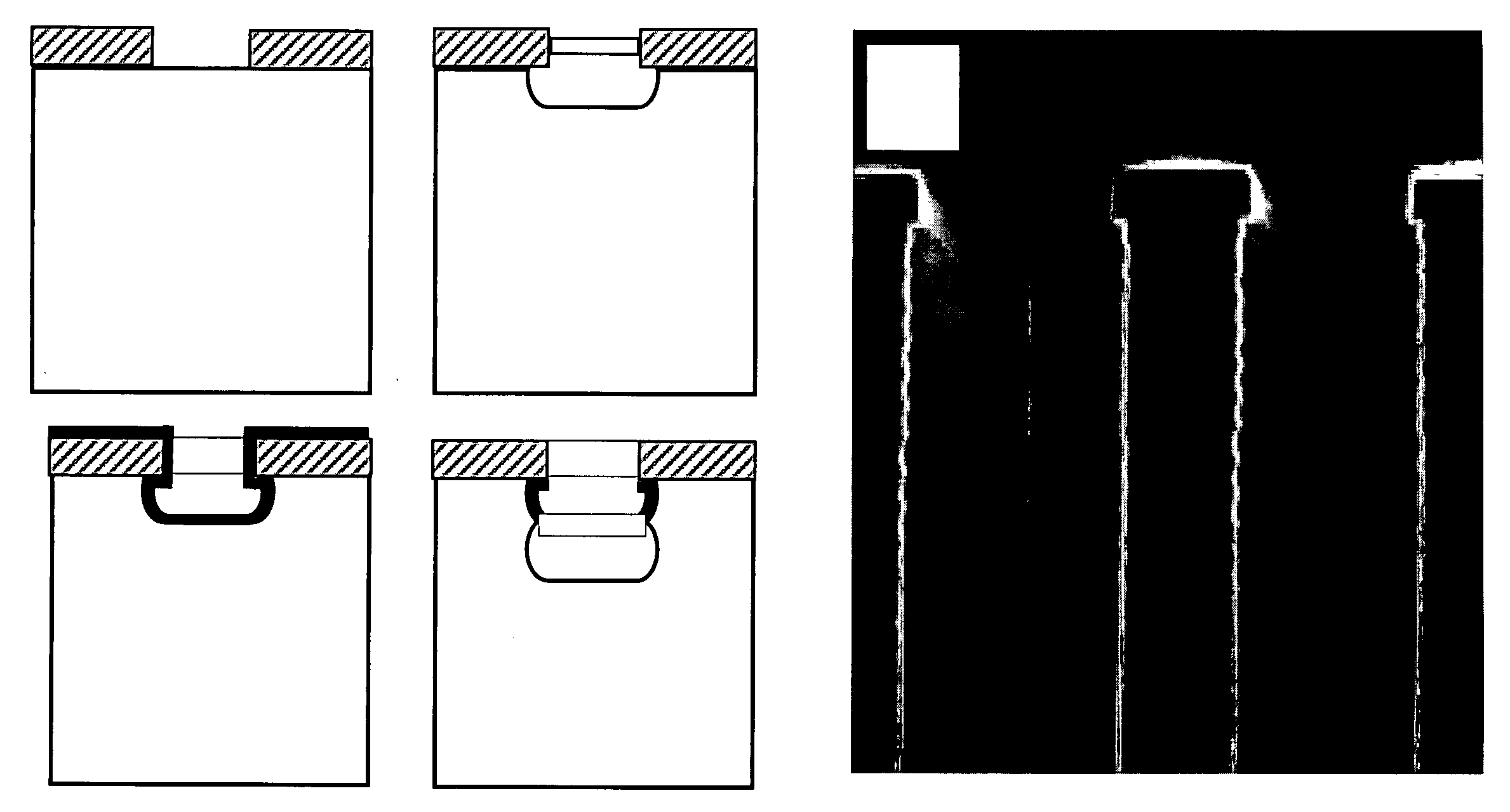
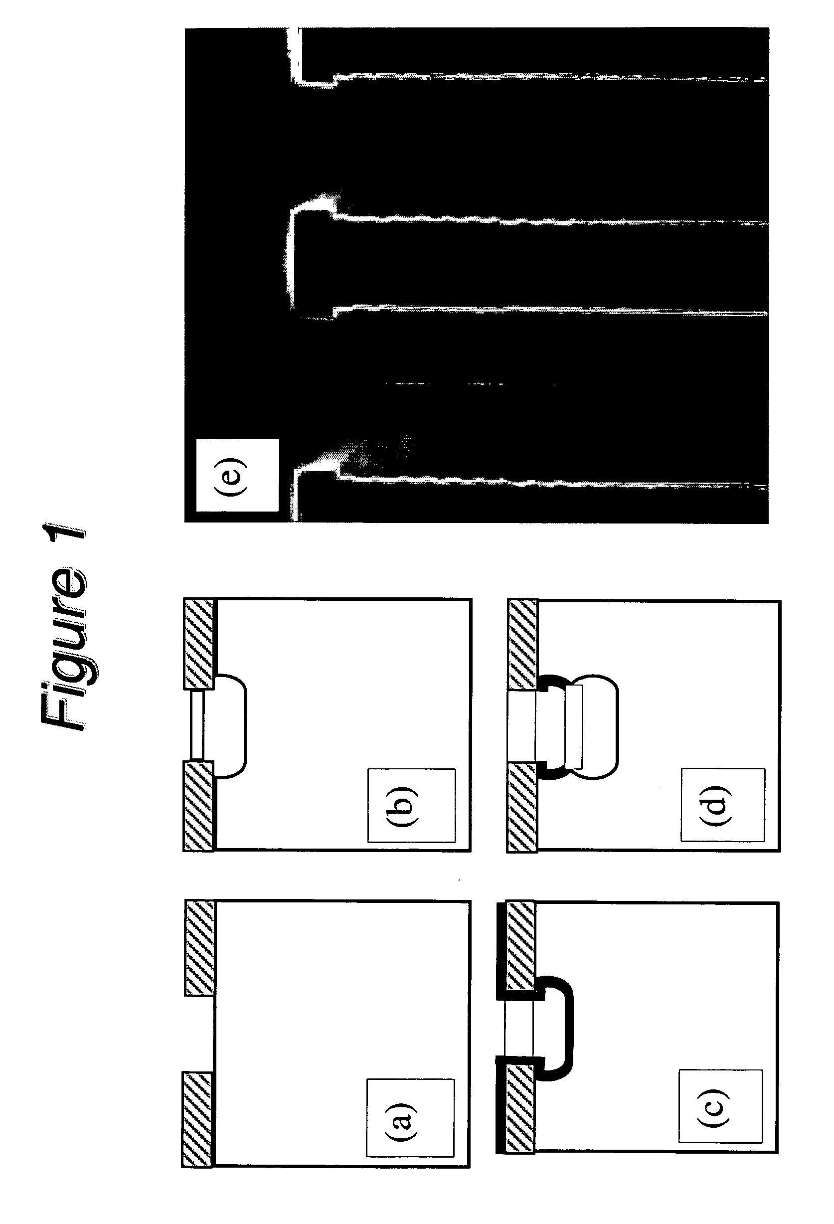
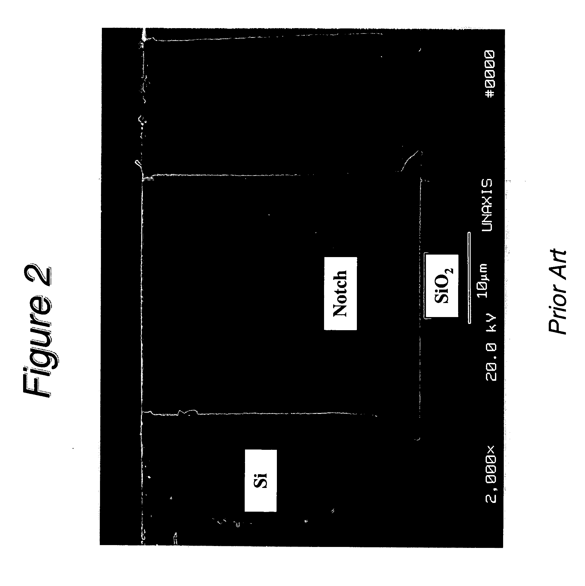
[0056] The result of etching an SOI structure using a standard TDM etch process (prior art) with an approximate 2 minute over-etch (sufficient to etch other smaller structures) is shown in the cross section of FIG. 2. The notch at the silicon-insulator interface is evident, and extends ˜3 μm into the silicon. Other features with widths of ˜4 μm were undercut to an extent that they were no longer attached to the substrate.

[0057] The preferred embodiment is a significant improvement over the prior art in terms of notch performance. The reactor is a commercially available Unaxis VLR modified according to the requirements of the present invention. FIG. 7 represents the preferred embodiment of the present invention, namely, frequency modulation of the RF bias for improved notch performance. The modulated RF bias is amplified and is applied through an impedance matching network to the electrode.

[0058] The test pattern used to characterize the notch performance has ˜45 μm of Si before a ...


PUM


Abstract

The present invention provides a method and an apparatus for reducing, or eliminating, the notching observed in the creation of SOI structures on a substrate when plasma etching through an alternating deposition / etch process by modulating the RF bias that is applied to the cathode. Modulation of the bias voltage to the cathode is accomplished either discretely, between at least two frequencies, or continuously during the alternating deposition / etch process.

Description

CROSS REFERENCES TO RELATED APPLICATIONS [0001] This application claims priority from and is related to commonly owned U.S. Provisional Patent Application Ser. No. 60 / 512933 filed Oct. 21, 2003, entitled: Notch-Free Etching of High Aspect SOI Structures Using a Time Division Multiplex Process and RF Bias Modulation, this Provisional Patent Application incorporated by reference herein.FIELD OF THE INVENTION [0002] The present invention relates generally to the manufacture of silicon based micro-electro-mechanical-systems. More particularly, the present invention relates to the manufacture of high aspect ratio silicon structures using alternating deposition and etching steps with a modulated RF bias. BACKGROUND OF THE INVENTION [0003] The fabrication of high aspect ratio features in silicon is used extensively in the manufacture of microelectromechanical (MEMS) devices. Such features frequently extend completely through the silicon wafer and may require etching in excess of 500 μm int...

Claims


Application Information

Patent Timeline
Patent Type & Authority Applications(United States)
IPC IPC(8): H01L21/3065H01L21/762
CPCH01L21/76283H01L21/30655
Inventor JOHNSON, DAVIDWESTERMAN, RUSSELLSRINIVASAN, SUNIL
Owner PLASMA THERM
Why Eureka
Try Eureka