
Switch LDMOS device and manufacturing method thereof

A device and switch technology, which is applied in the design and manufacture of semiconductor devices, can solve the problems of difficulty in increasing the breakdown voltage and large device size, and achieve the effects of reducing the channel length, reducing the device size, and optimizing the electric field distribution at the drain terminal

Pending Publication Date: 2020-07-03
SHANGHAI HUAHONG GRACE SEMICON MFG CORP
View PDF4 Cites 0 Cited by
  • Summary
  • Abstract
  • Description
  • Claims
  • Application Information

AI Technical Summary

Problems solved by technology

[0013] The technical problem to be solved by the present invention is to provide a switching LDMOS device to improve the problem that its breakdown voltage is difficult to increase and the device size is too large

Method used


Image

  • Switch LDMOS device and manufacturing method thereof
  • Switch LDMOS device and manufacturing method thereof
  • Switch LDMOS device and manufacturing method thereof

Examples


Embodiment 2

[0069] In the second embodiment, a P-type body region is also formed by ion implantation at the source end, therefore, the entire device has a body region at the periphery of the source region and the drain region. In the above two embodiments, the first doped body region 2 and the second doped body region 9 are both formed by self-aligned implantation.

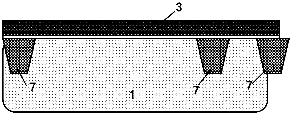
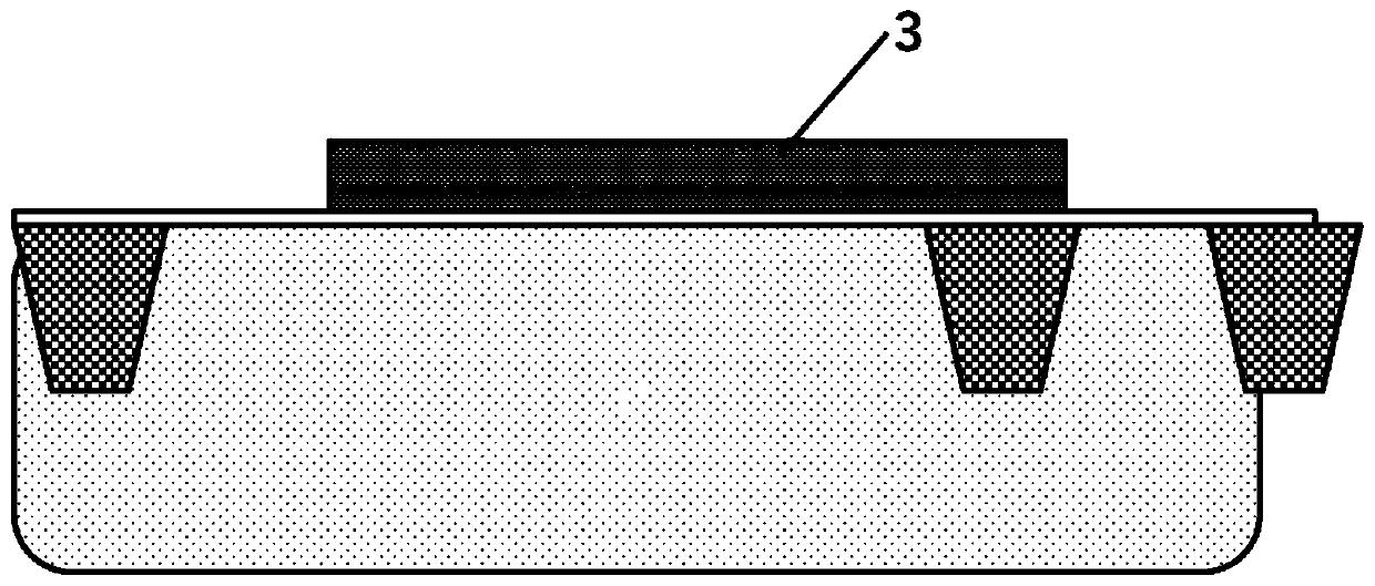
[0070] A method for manufacturing a switch LDMOS device according to the present invention, for the structure of Embodiment 1, refer to Figure 2-8 , including the following process steps:

[0071] Step 1, providing a semiconductor substrate, such as figure 2 As shown, an active region is formed on the semiconductor substrate, and the active region is used to form a switch LDMOS device; then ion implantation is performed in the active region to make a well region of the switch LDMOS device; field oxygen is formed; An oxide layer is deposited on the surface of the semiconductor substrate, and then a polysilicon layer is dep...


PUM

PropertyMeasurementUnit
breakdown voltageaaaaaaaaaa

Abstract

The invention discloses a switching LDMOS device. According to the invention, an LDD region of the switching LDMOS device and a first bulk-doped region of a second conduction type are arranged in a first trap in a semiconductor substrate; a first heavily-doped region serving as a source region is arranged in the LDD region, and a second heavily-doped region serving as a drain region is arranged inthe first bulk-doped region; in a gate structure, a channel of the switching LDMOS device is formed on the surface layer of the part, located between the LDD region and the bulk-doped region, of thesemiconductor substrate, and when a voltage applied to a gate exceeds the threshold voltage of the LDMOS device, the channel is inverted, so the source region and the drain region are conducted; and one side, far away from the gate structure, of each of the LDD region and the bulk-doped region is provided with field oxygen or STI, and one side of the field oxygen or STI is connected with the firstheavily-doped region in the LDD or the second heavily-doped region in the first bulk-doped region. With the bulk-doped region having higher ion implantation energy and ion implantation dosage, the purposes of improving the breakdown voltage (BV) of the device and reducing the size of the device are achieved.

Description

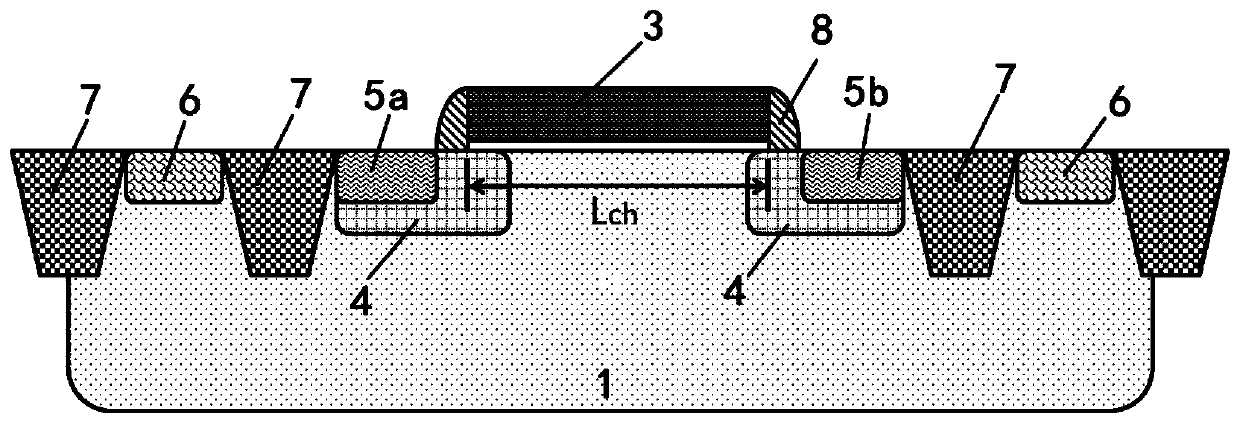
technical field [0001] The invention relates to the field of semiconductor device design and manufacture, in particular to a switch LDMOS device, and the invention also relates to a manufacturing method of the switch LDMOS device. Background technique [0002] At present, 5V switching LDMOS devices adopt the conventional structure of CMOS, such as figure 1 As shown, taking the most common N-type LDMOS device structure as an example, figure 1 Only some key structures are shown in the figure, there is an LDD region in the P well, the source region and the drain region of the switching LDMOS device are respectively located in the LDD region, the channel region is between the two LDD regions, and the two The substrate surface between the LDD regions has the gate structure of the switching LDMOS device composed of a gate oxide layer and a polysilicon gate, and the gate structure also has gate spacers on both sides along the channel length direction. [0003] The surface of the ...

Claims


Application Information

Patent Timeline
Patent Type & Authority Applications(China)
IPC IPC(8): H01L29/78H01L29/06H01L29/08H01L21/336
CPCH01L29/7816H01L29/0619H01L29/086H01L29/0878H01L29/66681H01L29/7835H01L29/66659H01L29/0653H01L29/1087H01L29/1045H01L29/66484H01L29/66492H01L29/66689H01L29/7831
Inventor 杨新杰金锋乐薇张晗宋亮
Owner SHANGHAI HUAHONG GRACE SEMICON MFG CORP
Learn More