
LDMOS transistor and preparation method thereof

A transistor and semiconductor technology, used in semiconductor/solid-state device manufacturing, semiconductor devices, electrical components, etc., can solve the problems of conflicting on-resistance performance requirements, high breakdown voltage and low breakdown voltage, etc., to improve the breakdown voltage BV, reduce the conduction On-resistance, the effect of improving the breakdown voltage

Pending Publication Date: 2021-12-24
SIEN QINGDAO INTEGRATED CIRCUITS CO LTD
View PDF0 Cites 2 Cited by
  • Summary
  • Abstract
  • Description
  • Claims
  • Application Information

AI Technical Summary

Problems solved by technology

[0004] In view of the above-mentioned shortcomings of the prior art, the object of the present invention is to provide an LDMOS transistor and a preparation method thereof, which are used to solve the problem that the LDMOS transistor device in the prior art adopts an STI structure in the drift region to increase the breakdown voltage. Bringing problems such as the contradiction between high breakdown voltage and low on-resistance performance requirements of LDMOS transistor devices

Method used


Image

  • LDMOS transistor and preparation method thereof
  • LDMOS transistor and preparation method thereof
  • LDMOS transistor and preparation method thereof

Examples


Embodiment 1

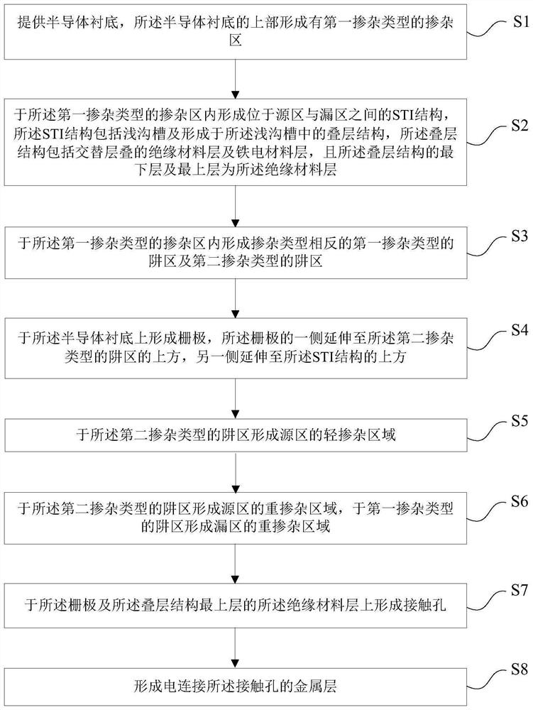
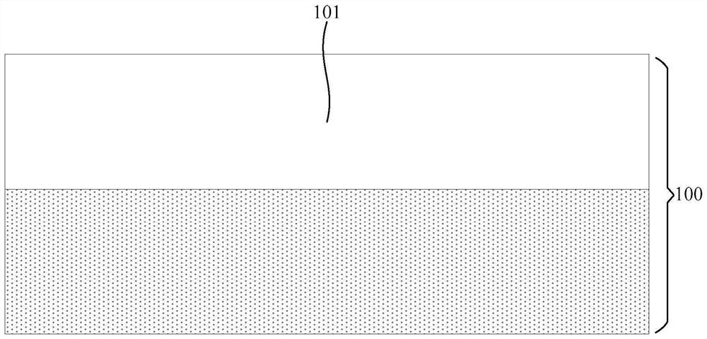
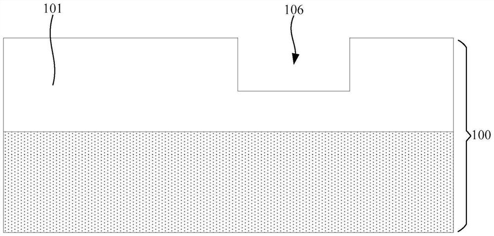
[0069] This embodiment provides a method for preparing an LDMOS transistor. For ease of understanding, this embodiment is described by taking the method for preparing an N-type LDMOS transistor as an example. Those skilled in the art can change the doping type of the transistor as needed to obtain A method for preparing a P-type LDMOS transistor with the same structure.

[0070] Taking the N-type LDMOS transistor as an example, a capacitor structure is formed between the gate and the drain by setting a contact hole and a metal layer between the gate and the STI structure. When the transistor is in the on state, the gate voltage is high, Additional electrons can be induced under the insulating material layer (LDMOS drift region) in the STI structure, thereby reducing the on-resistance Ron, and when the transistor is in the off state, the gate voltage is grounded, and the contact hole will be in the STI structure. An additional depletion region is induced under the insulating ma...

Embodiment 2

[0094] This embodiment provides an LDMOS transistor. The LDMOS transistor can be prepared by the preparation method of the first embodiment above, but is not limited to the preparation method described in the first embodiment, as long as the LDMOS transistor can be formed. For the beneficial effects achieved by the LDMOS transistor, please refer to Embodiment 1, and details will not be repeated below. In addition, the following embodiments are described by taking an N-type LDMOS transistor as an example, and those skilled in the art can change the doping type of the transistor as required to obtain a P-type LDMOS transistor with the same structure.

[0095] Such as Figure 11 shown, the LDMOS transistor consists of:

[0096] A semiconductor substrate 100, an N-type doped region 101 is formed on the upper part of the semiconductor substrate 100, and an N-type well region 102 and a P-type well region 103 with opposite doping types are formed in the N-type doped region 101;

[...


PUM


Abstract

The invention provides an LDMOS (Laterally Diffused Metal Oxide Semiconductor) transistor and a preparation method thereof. The transistor comprises a semiconductor substrate in which a doping region of a first doping type is formed, and a well region of the first doping type and a well region of a second doping type which are opposite in doping type are formed in the doping region of the first doping type; a source region is positioned in the well region of the second doping type; the drain region is positioned in the well region of the first doping type; an STI structure is located between the source region and the drain region, the STI structure comprises a laminated structure formed in the shallow trench, and the laminated structure comprises insulating material layers and ferroelectric material layers which are alternately laminated; a grid electrode is located on the semiconductor substrate, one side of the grid electrode extends to the upper part of the source region, and the other side of the grid electrode extends to the upper part of the STI structure; a contact hole is connected with the grid electrode and the insulating material layer on the uppermost layer of the laminated structure; a metal layer is electrically connected with the contact hole. According to the LDMOS transistor, the breakdown voltage BV of an LDMOS transistor device is improved, and meanwhile the on-resistance Ron of the LDMOS transistor device is effectively reduced.

Description

technical field [0001] The invention relates to the field of double diffused metal oxide semiconductor (DMOS), in particular to an LDMOS transistor and a preparation method thereof. Background technique [0002] In power device applications, since DMOS (double-diffused metal-oxide-semiconductor) technology adopts a vertical device structure (such as a vertical NPN bipolar transistor), it has many advantages, including high current drive capability, low on-resistance Ron and high Breakdown voltage BV etc. There are two main types of DMOS transistors, vertical double diffused metal oxide semiconductor field effect transistor VDMOS and lateral double diffused metal oxide semiconductor field effect transistor LDMOS. Compared with common field effect transistors, LDMOS transistors have obvious advantages in terms of key device characteristics, such as gain, linearity, switching performance, heat dissipation performance, and reduction of stages. At the same time, LDMOS transistor...

Claims


Application Information

Patent Timeline
Patent Type & Authority Applications(China)
IPC IPC(8): H01L29/06H01L29/78H01L21/762H01L21/336
CPCH01L29/7816H01L29/66681H01L29/0611H01L21/76224H01L29/0649H01L29/66689H01L29/0653H01L29/0878H01L29/407H01L29/7824H01L29/78391
Inventor 李敏季明华张汝京
Owner SIEN QINGDAO INTEGRATED CIRCUITS CO LTD
Learn More