
High-voltage device of mixed junction terminal protection structure comprising ferroelectric material and preparation method of high-voltage device

A technology of protection structure and ferroelectric material, which is applied in semiconductor/solid-state device manufacturing, electrical components, semiconductor devices, etc., can solve the problems of large area of ​​terminal protection structure, increased on-resistance, complicated process, etc. The effect of reducing on-resistance and simple process steps

Pending Publication Date: 2021-12-24
SIEN QINGDAO INTEGRATED CIRCUITS CO LTD
View PDF4 Cites 0 Cited by
  • Summary
  • Abstract
  • Description
  • Claims
  • Application Information

AI Technical Summary

Problems solved by technology

[0004] In view of the above-mentioned shortcomings of the prior art, the object of the present invention is to provide a high-voltage device and a preparation method of a hybrid junction termination protection structure containing ferroelectric materials, which are used to solve the problem of junction termination protection structures of high-voltage semiconductor devices in the prior art. When increasing the breakdown voltage of the device, there are problems such as complex process, large area of ​​terminal protection structure, high cost or increased on-resistance.

Method used


Image

  • High-voltage device of mixed junction terminal protection structure comprising ferroelectric material and preparation method of high-voltage device
  • High-voltage device of mixed junction terminal protection structure comprising ferroelectric material and preparation method of high-voltage device
  • High-voltage device of mixed junction terminal protection structure comprising ferroelectric material and preparation method of high-voltage device

Examples


Embodiment 1

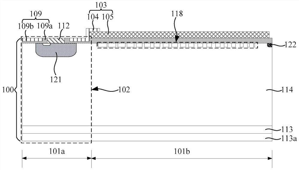
[0075] Such as figure 1 As shown, this embodiment provides a high-voltage device with a hybrid junction terminal protection structure containing ferroelectric materials, and the high-voltage semiconductor device includes:

[0076] forming an active region 101a with a high voltage semiconductor device 102;

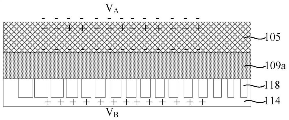
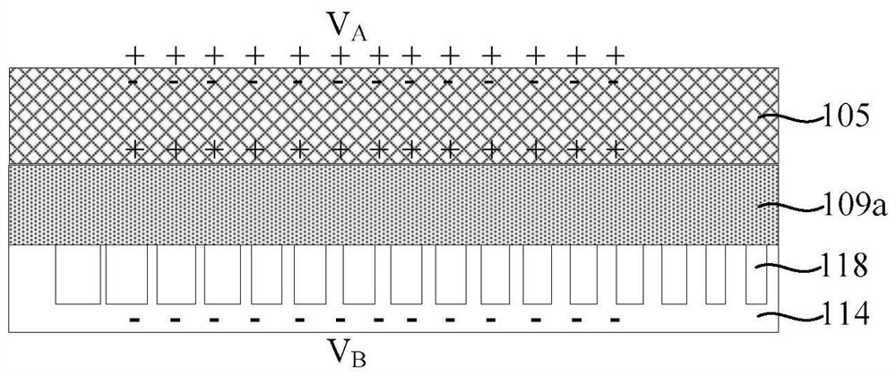
[0077] A hybrid junction termination protection structure having a RESURF structure 103 including a first bias field plate 104 electrically connected to the active region 101a and located below the first bias field plate 104 and connected to the The first bias field plate 104 contacts the ferroelectric material layer 105 .

[0078] What needs to be explained here is that the function of the hybrid junction terminal protection structure described in this embodiment is consistent with the function of existing high-voltage power device products, both of which are to prevent the device from breaking down in advance at the edge of the main PN junction to increase the withstand ...


PUM


Abstract

The invention provides a high-voltage device of a mixed junction terminal protection structure comprising a ferroelectric material and a preparation method. The device comprises an active region, wherein ahigh-voltage semiconductor device is formed in the active region; a hybrid terminal protection structure with an RESURF structure; wherein the RESURF structure comprises a first bias field plate which is electrically connected with the active region and a ferroelectric material layer which is positioned below the first bias field plate and is in contact with the first bias field plate. According to the high-voltage semiconductor device structure, the breakdown voltage BV of a device can be further improved on the basis of an existing junction terminal protection structure. Meanwhile, the on resistance Ron of the device is effectively reduced, and miniaturization of the device structure is easier to achieve; in addition, the preparation process of the device can be realized only by adding a conventional deposition process and a photoetching process on the basis of an existing device preparation process, and the process steps are simple and easy to realize.

Description

technical field [0001] The invention relates to the technical field of high-voltage semiconductor devices, in particular to a high-voltage device and a preparation method of a hybrid junction terminal protection structure containing ferroelectric materials. Background technique [0002] The ability of high-voltage power semiconductor devices to block high voltage is mainly limited by the withstand voltage capability of the PN junction of edge cells. At present, a shallow planar junction structure is generally used. Due to the PN junction manufactured by a planar process, the dopant ions are diffused in the corner area of ​​​​the photolithographic mask window to form a cylindrical junction and a spherical junction. Due to the curvature of these two junctions, As a result of electric field concentration, avalanche breakdown first occurs in these areas, thereby reducing the breakdown voltage of the PN junction. At the same time, due to the influence of interface charges, the s...

Claims


Application Information

Patent Timeline
Patent Type & Authority Applications(China)
IPC IPC(8): H01L29/06H01L29/40H01L29/739H01L29/78H01L21/336H01L21/331
CPCH01L29/063H01L29/7398H01L29/7823H01L29/7811H01L29/404H01L29/66333H01L29/66681H01L29/66712H01L29/402H01L29/7395H01L29/0623H01L29/7816H01L29/0878H01L29/861H01L29/7813H01L29/66734H01L29/0619H01L29/0649H01L29/1608H01L29/2003H01L29/408H01L29/7397H01L29/43H01L29/1095
Inventor 季明华李敏张汝京
Owner SIEN QINGDAO INTEGRATED CIRCUITS CO LTD
Learn More