
Analog switching circuit

A technology for simulating switching circuits and switching tubes, applied in electronic switches, electrical components, pulse technology, etc., can solve problems such as decreased integration and increased energy consumption

Active Publication Date: 2012-07-11
CRM ICBG (WUXI) CO LTD
View PDF0 Cites 0 Cited by
  • Summary
  • Abstract
  • Description
  • Claims
  • Application Information

AI Technical Summary

Problems solved by technology

However, expanding the size of MOS devices will inevitably lead to a series of side effects such as a decrease in integration and increased energy consumption. Therefore, simply increasing the size of the device has great limitations.

Method used


Image

  • Analog switching circuit
  • Analog switching circuit
  • Analog switching circuit

Examples


Embodiment Construction

[0012] A specific embodiment of the present invention will be described in detail below in conjunction with the accompanying drawings.

[0013] First look at the MOS tube impedance formula of the analog switch circuit in the prior art:

[0014] Rds = L K * W * ( V gs - V TH - V ds )

[0015] Among them, K is a fixed coefficient, Vgs and Vds are the gate-source voltage and drain-source voltage of the MOS transistor respectively, which are determined by the input terminal voltage and the control terminal voltage. In addition to reducing Rds by increasing W / L, It can also be realized by lowering the...


PUM


Abstract

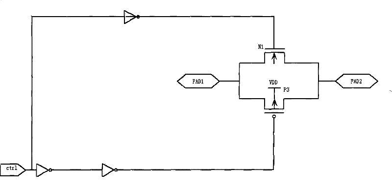
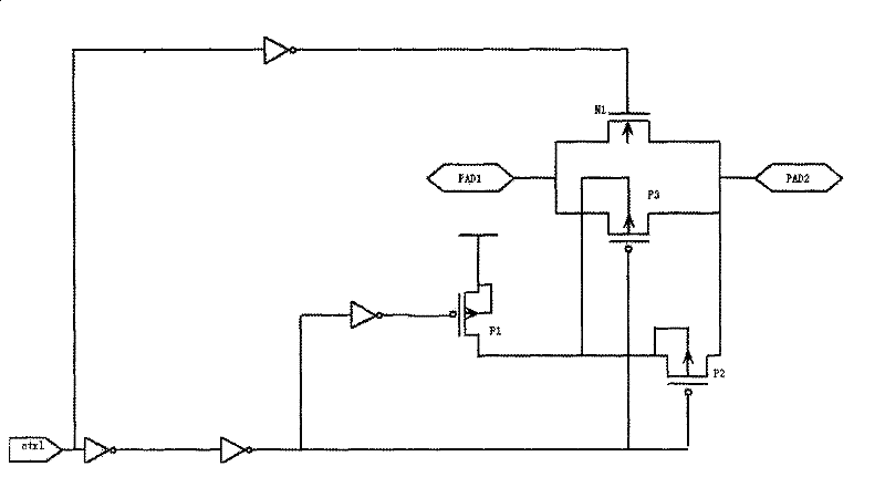
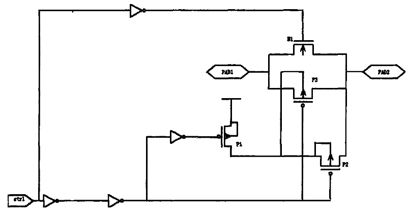
The invention provides an analog switching circuit with low impedance, comprising two enhanced metal oxide semiconductor (MOS) switching tubes (P3) and (N1) connected in parallel, source electrodes of both enhanced MOS switching tubes are together used as input ends, and drain electrodes are together used as output ends; and the substrate of the switching tube (P3) is connected with two transmission tubes in parallel, is connected with a power supply level (VDD) through the transmission tube (P1) and is connected with the input end of the switching tube (N1) through the transmission tube (P2). When an analog switch is turned on, the substrate of the switching tube P3 is connected with the input end, namely the source electrode, so that the bias voltage of the substrate is zero, the threshold voltage Vth of the substrate is reduced, and then the purpose of reducing the impedance Rds is achieved; and therefore, the turning-on impedance of the whole analog switch can be further reduced without enlarging the size of elements.

Description

【Technical field】 [0001] The invention relates to a CMOS process analog switch, in particular to an analog switch circuit with low conduction resistance. 【Background technique】 [0002] In integrated circuit design, analog switches are often used to switch paths during signal transmission. The most common usage is to use the clock signal to control the on-off of the analog switch, so that the input signal at the input terminal is periodically derived from the output terminal. Generally, it is hoped that during signal transmission, its attenuation is as small as possible. Reflected on the analog switch, the voltage drop of the input signal is lower after passing through the switch, which is generally achieved by reducing the on-resistance of the analog switch as much as possible. [0003] Such as figure 1 As shown, this is an existing standard CMOS process analog switch circuit. Its basic structure is that NMOS and PMOS are connected in parallel. Obviously, the on-resista...

Claims


Application Information

Patent Timeline
Patent Type & Authority Patents(China)
IPC IPC(8): H03K17/687
Inventor 朱立群傅建军罗先才徐兴明徐栋胡燕
Owner CRM ICBG (WUXI) CO LTD
Learn More