
Irradiation-reinforced SiC super-junction MOS structure

Pending Publication Date: 2022-02-15
BEIJING UNIV OF TECH
View PDF0 Cites 0 Cited by
  • Summary
  • Abstract
  • Description
  • Claims
  • Application Information

AI Technical Summary

Problems solved by technology

However, it is still affected by the radiation effect when applied in environments such as single particle irradiation, which seriously affects its application in the aerospace field.

Method used


Image

  • Irradiation-reinforced SiC super-junction MOS structure
  • Irradiation-reinforced SiC super-junction MOS structure

Examples


Embodiment 1

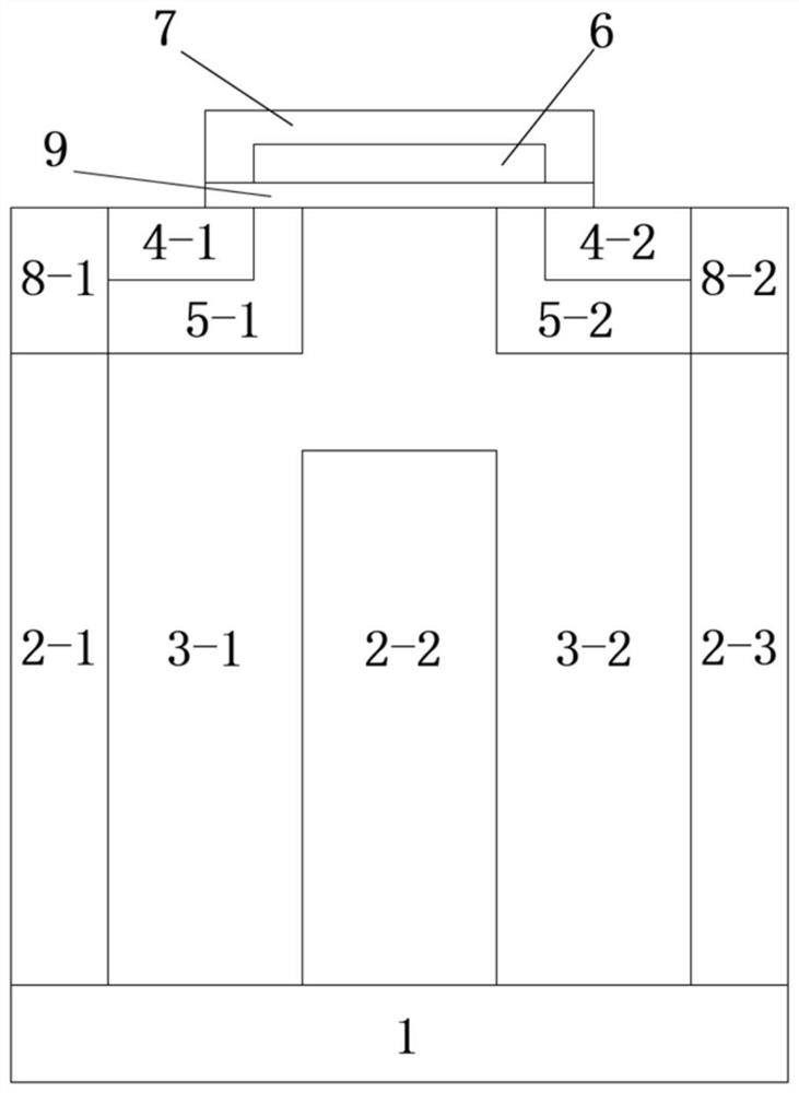
[0022] A radiation-hardened SiC superjunction MOS structure in this embodiment includes:

[0023] N+ drain region(1);

[0024] P column is divided into three parts (2-1), (2-2), (2-3), N column is divided into two parts (3-1), (3-2), and (2-1), (3-1), (2-2), (3-2), and (2-3) are arranged alternately in sequence, and are located on the upper surface of the N+ drain region (1);

[0025] The P-base area (5) is divided into left and right parts, the left P-base area (5-1) is located on the upper surface of the N-pillar (3-1), and the right P-base area (5-2) , located on the upper surface of the N pillar (3-2);

[0026] The N-source area (4) is divided into left and right parts, the left side N-source area (4-1) is located on the upper surface of the preset area of ​​the P-base area (5-1), and the right side N-source area the area (4-2), located on the upper surface of the preset area of ​​the P-base area (5-2);

[0027] The P-plus area (8) is divided into left and right parts,...


PUM

PropertyMeasurementUnit
Thicknessaaaaaaaaaa
Thicknessaaaaaaaaaa

Abstract

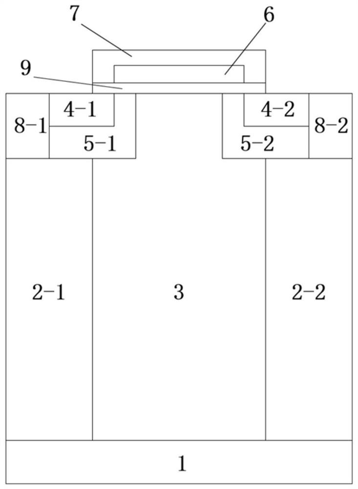
The invention provides an irradiation-reinforced SiC super-junction MOS structure, which sequentially comprises the following parts from bottom to top: an N + drain region, wherein P columns and N columns are alternately arranged on the upper surface of the N + drain region; a left side P-base region, a right side P-base region, a left side N-source region and a right side N-source region that are located on the upper surface of the P-base 5; a left P column, a middle P column and a right P column that are connected into a whole in the chip and are connected with a left P-plus area and a right P-plus area; a gate oxide that is located in a partial region of the left side N-source region, a partial region of the right side N-source region, a partial region of the preset region of the left side P-base region, a partial region of the preset region of the right side P-base region and the upper surface of a part of N columns; and a polysilicon gate that is located between the gate oxide and an isolation oxide, wherein the gate oxide is located at the uppermost end. The invention has the advantages of being high in radiation resistance, low in gate-drain capacitance, low in switching loss and high in short-circuit capacity.

Description

technical field [0001] The invention relates to the technical field of semiconductors, in particular to a radiation-strengthened SiC superjunction MOS structure. Background technique [0002] The proposal of the superjunction structure effectively improves the compromise between the breakdown voltage and on-resistance of MOS devices. It uses P-type and N-type semiconductor materials to alternate with each other, which can make the electric field distribution more uniform when the device is off, thereby effectively improving the performance of the device. The withstand voltage, so low-resistance epitaxial wafers can be used to achieve lower on-resistance requirements. For SiC super junction MOS, it has all the advantages of SiC devices at the same time, so it is the most promising power semiconductor device in the future. However, when applied in environments such as single particle irradiation, it is still affected by the radiation effect, which seriously affects its applic...

Claims


Application Information

Patent Timeline
IPC IPC(8): H01L29/78H01L29/06H01L29/16H01L29/167H01L29/423
CPCH01L29/0634H01L29/7827H01L29/42356H01L29/1608H01L29/167H01L29/7802
Inventor 周新田张仕达贾云鹏胡冬青吴郁
Owner BEIJING UNIV OF TECH
Learn More