rf LDMOS device and manufacturing method

A device, N-type technology, applied in semiconductor/solid-state device manufacturing, semiconductor devices, electrical components, etc., can solve problems such as complex manufacturing process, achieve simple device manufacturing process, improve breakdown voltage, high breakdown voltage effect

Active Publication Date: 2015-08-19
SHANGHAI HUAHONG GRACE SEMICON MFG CORP
View PDF6 Cites 0 Cited by
  • Summary
  • Abstract
  • Description
  • Claims
  • Application Information

AI Technical Summary

Problems solved by technology

However, in the manufacturing process of RF LDMOS with two or more metal layers, the Faraday shield needs to be made with two (or more) metal layers, at least two metal layer deposition and etching processes are required, and the manufacturing process is complicated.

Method used


Image

  • rf LDMOS device and manufacturing method
  • rf LDMOS device and manufacturing method
  • rf LDMOS device and manufacturing method

Examples


Embodiment 1

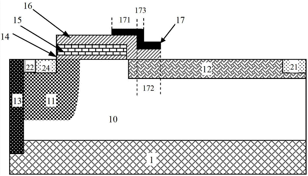
[0046] The structure of RF LDMOS device is as Figure 4 shown. An N-type drain end lightly doped drift region 12 is formed on the right part of the P epitaxy 10, and a gate oxide 14 is formed on the P epitaxy 10 on the left side of the N-type drain end lightly doped drift region 12, above the gate oxide 14 A polysilicon gate 15 is formed, a dielectric layer 16 is formed on the top of the polysilicon gate 15, on the side and on the left part of the lightly doped drift region 12 of the N-type drain, and a Faraday shield is formed on the right part of the dielectric layer 16. shield) 17, the Faraday shield 17 is a single-layer metal layer, the single-layer metal layer includes a polysilicon portion 171, a drift portion 172, and a vertical portion 173, the vertical portion 173 is on the right side of the polysilicon gate 15, and the upper end of the vertical portion 173 It communicates with the right end of the polysilicon part 171, the lower end of the vertical part 173 communic...

Embodiment 2

[0050] Based on Embodiment 1, the structure of the RF LDMOS device is as follows Figure 4 shown. A P well 11 is formed on the left part of the P epitaxy 10, and an N-type drain terminal lightly doped drift region 12 is formed on the right part of the P epitaxy 10, and the P well 11 and the N-type drain terminal lightly doped drift region are formed. 12 no contact;

[0051] An N-type source terminal heavily doped region 24 is formed on the upper part of the P well 11;

[0052] An N-type drain heavily doped region 21 is formed in the right part of the N-type drain lightly doped drift region 12;

[0053] The N-type impurity concentration of the N-type source heavily doped region 24 and the N-type drain heavily doped region 21 is greater than the N-type impurity concentration of the N-type drain lightly doped drift region 12;

[0054] Above the P well 11 on the right side of the N-type source heavily doped region 24, and above the P epitaxy 10 between the P well 11 and the N-t...

Embodiment 3

[0056] The manufacturing method of the RF LDMOS device described in embodiment one, comprises the following steps:

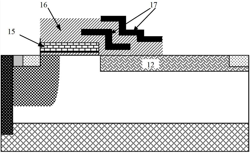
[0057] 1. Form gate oxide 14, polysilicon gate 15, N-type drain lightly doped drift region 12, N-type drain lightly doped drift region 12 is formed on the right part of P epitaxy 10, gate oxide 14 is formed on N-type drain On the P epitaxy 10 on the left side of the lightly doped drift region 12, a polysilicon gate 15 is formed on the gate oxide 14, as Figure 5 shown;

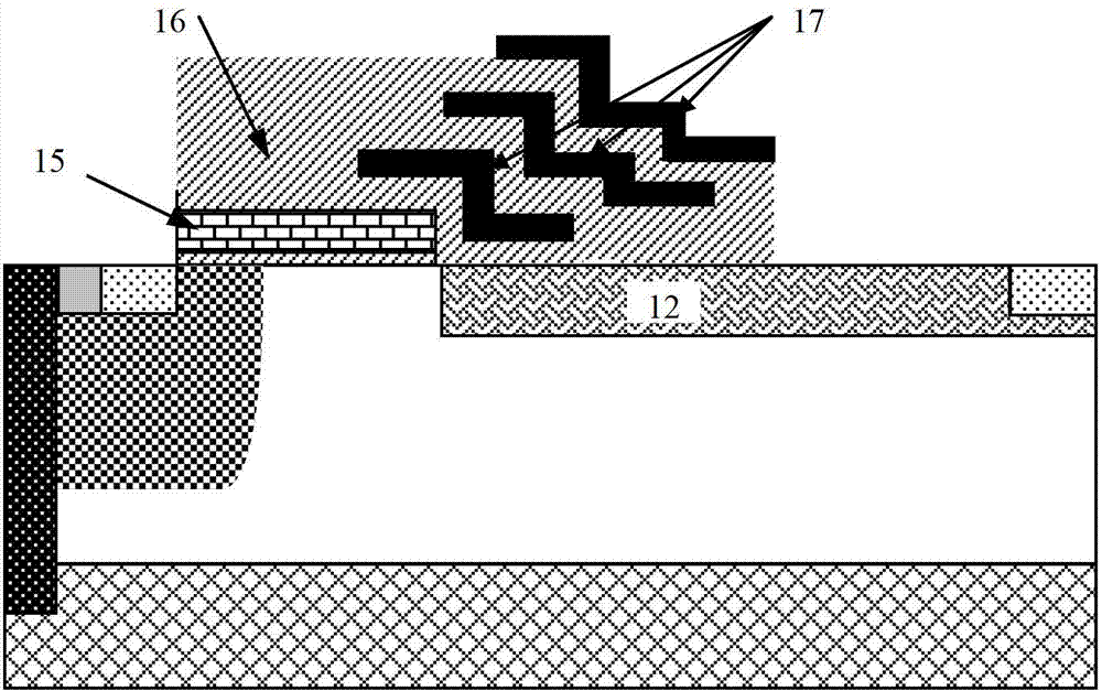
[0058] two. A layer of silicon oxide 16 is integrally deposited on the silicon wafer, such as Image 6 shown; preferably, the thickness of the layer of silicon oxide is 1000-4000 angstroms;

[0059] three. By photolithography, a groove is formed in the silicon oxide above the left part of the lightly doped drift region of the N-type drain, and the depth of the groove is smaller than the thickness of the layer of silicon oxide 16, such as Figure 7 shown; preferably, the width of the trench ...


PUM

PropertyMeasurementUnit
thicknessaaaaaaaaaa
depthaaaaaaaaaa
breakdown voltageaaaaaaaaaa

Abstract

The invention discloses an RF LDMOS (ratio frequency laterally diffused metal oxide semiconductor) device, which is structurally characterized in that a Faraday shield is a single-layer metal layer, the single-layer metal layer comprises a polycrystalline silicon part, a drifting part and a vertical part, the vertical part is arranged at the right side of a polycrystalline silicon grid, the upper end of the vertical part is communicated with the right end of the polycrystalline silicon part, the lower end of the vertical part is communicated with the left end of the drifting part, the left end of the polycrystalline silicon part is positioned above the polycrystalline silicon grid, the drifting part is positioned above an N type drain end light doping drifting region, a medium layer positioned right under the polycrystalline silicon part is silicon oxide, a medium layer positioned right under the drifting part comprises silicon oxide and silicon nitride, the width of the silicon nitride region is smaller than the width of the drifting part, the upper part of the silicon nitride region is connected with the drifting part of the single-layer metal layer, and silicon oxide is arranged at the lower part and the two sides. The invention also discloses a manufacture method of the RF LDMOS device. The RF LDMOS device has higher breakdown voltage, and in addition, the manufacture process is simple.

Description

technical field [0001] The invention relates to semiconductor technology, in particular to an RF LDMOS device and a manufacturing method thereof. Background technique [0002] RF LDMOS (Radio Frequency Laterally Diffused Metal Oxide Semiconductor) device is a new generation of integrated solid microwave power semiconductor product that is a fusion of semiconductor integrated circuit technology and microwave electronic technology. It has good linearity, high gain, high withstand voltage, and output power. Large size, good thermal stability, high efficiency, good broadband matching performance, easy to integrate with MOS process, etc., and its price is much lower than that of gallium arsenide devices. It is a very competitive power device and is widely used in GSM , PCS, W-CDMA base station power amplifier, and wireless broadcasting and nuclear magnetic resonance, etc. [0003] In the design process of RF LDMOS, a small on-resistance and a large breakdown voltage are required...

Claims


Application Information

Patent Timeline
Patent Type & Authority Patents(China)
IPC IPC(8): H01L29/78H01L29/40H01L21/336
Inventor 李娟娟慈朋亮钱文生韩峰董金珠
Owner SHANGHAI HUAHONG GRACE SEMICON MFG CORP
Why Eureka
Try Eureka