Nonvolatile memory and forming method thereof

A non-volatile, memory technology used in the semiconductor field to solve problems such as low erasing efficiency

Active Publication Date: 2020-07-07
NEXCHIP SEMICON CO LTD
View PDF4 Cites 2 Cited by
  • Summary
  • Abstract
  • Description
  • Claims
  • Application Information

AI Technical Summary

Problems solved by technology

[0013] The purpose of the present invention is to provide a non-volatile memory to solve the problem of low erasing efficiency in the existing non-volatile memory

Method used


Image

  • Nonvolatile memory and forming method thereof
  • Nonvolatile memory and forming method thereof
  • Nonvolatile memory and forming method thereof

Examples


Embodiment Construction

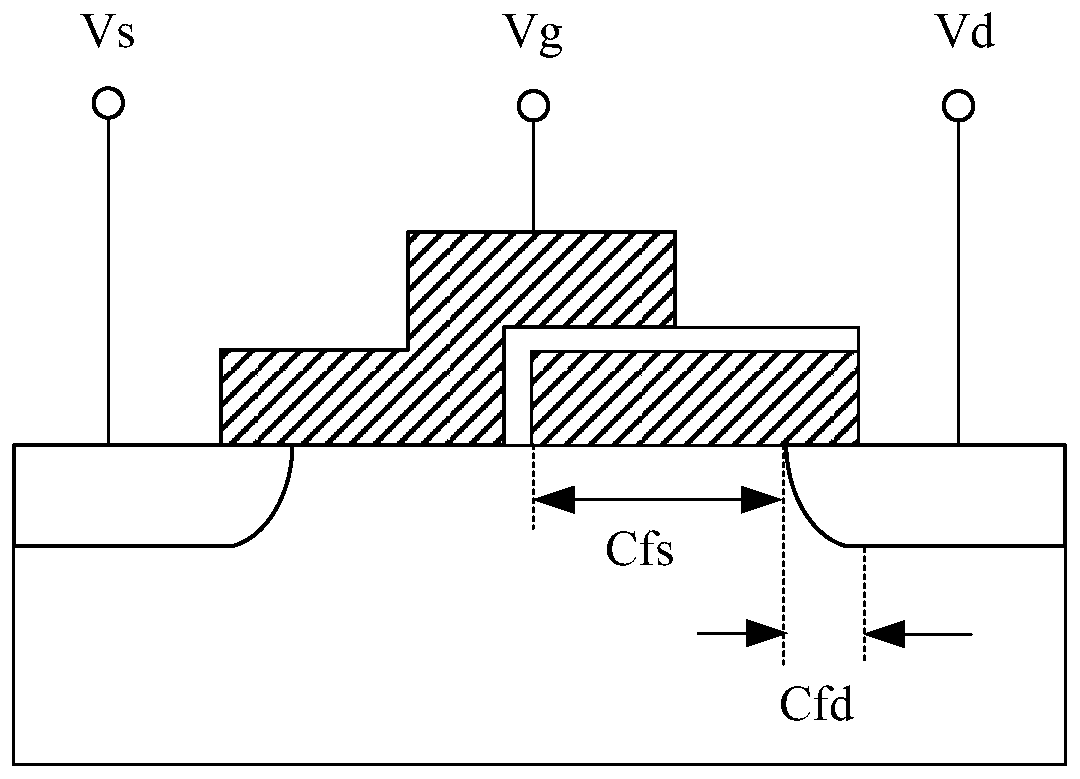
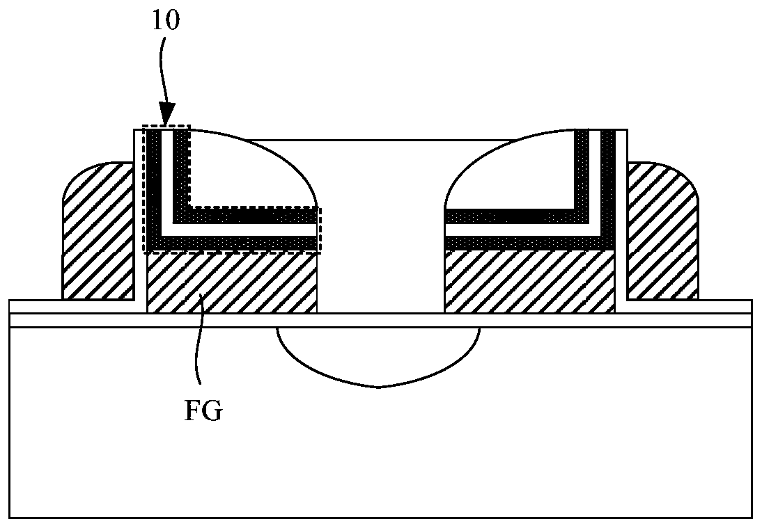
[0086] The non-volatile memory and its forming method proposed by the present invention will be further described in detail below with reference to the drawings and specific embodiments. The advantages and features of the present invention will become clearer from the following description. It should be noted that all the drawings are in a very simplified form and use imprecise scales, and are only used to facilitate and clearly assist the purpose of illustrating the embodiments of the present invention.

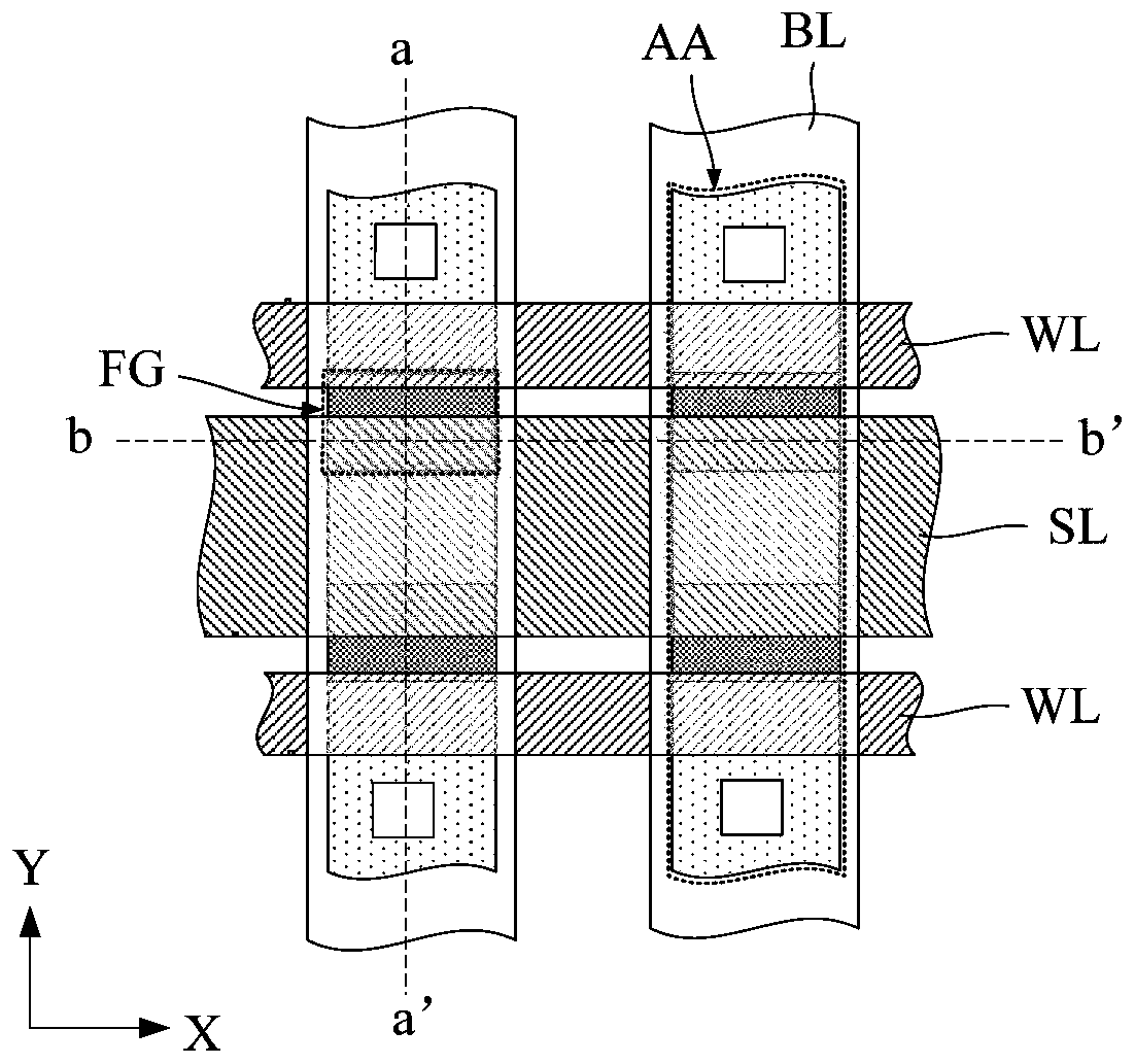
[0087] Figure 2a The layout structure of the non-volatile memory in an embodiment of the present invention, Figure 2b for Figure 2a The shown non-volatile memory corresponds to the cross-sectional schematic diagram of the aa' direction, Figure 2c for Figure 2a The shown non-volatile memory corresponds to a schematic cross-sectional view in the direction of bb'. Such as Figure 2a ~ Figure 2c As shown, the non-volatile memory includes:

[0088] At least one subst...


PUM


Abstract

The invention provides a nonvolatile memory and a forming method thereof. A first tip structure is formed on the top surface, close to a word line, of a floating gate to adjust the morphology of the end, close to the word line, of the floating gate, so that the end, close to the word line, of the floating gate is provided with a second tip structure. According to the nonvolatile memory formed based on the structure, when the nonvolatile memory executes the erasing operation, the electric field intensity of the floating gate at the second tip structure can be enhanced, so that electrons in thefloating gate can penetrate into a word line more favorably, and the erasing efficiency of the memory is effectively improved.

Description

technical field [0001] The invention relates to the technical field of semiconductors, in particular to a nonvolatile memory and a forming method thereof. Background technique [0002] Driven by application requirements, non-volatile memory (Non-Volatile Memory, NVM) develops rapidly. In various non-volatile memory products, it is capable of multiple data storage, reading, erasing, etc., and has become a memory element widely used in personal computers and electronic equipment. Generally, a floating gate is provided in a non-volatile memory, and the coupling ratio (coupling ratio, CR) between the floating gate and other components will directly affect the coupling to the floating gate. The size of the coupling voltage on the upper, and then will affect the operating efficiency of the non-volatile memory. [0003] For example, Figure 1a is a schematic structural diagram of an existing non-volatile memory, Figure 1a The nonvolatile memory shown includes a floating gate, a ...

Claims


Application Information

Patent Timeline
Patent Type & Authority Applications(China)
IPC IPC(8): H01L27/11521H01L27/11526H01L27/11531
CPCH10B41/42H10B41/40H10B41/30
Inventor 陈耿川
Owner NEXCHIP SEMICON CO LTD
Why Eureka
Try Eureka