Quantum dot light-emitting diode and preparation method thereof
A quantum dot light-emitting and diode technology, which is applied in the manufacture of semiconductor/solid-state devices, semiconductor devices, electrical components, etc., can solve the problems of orbital hybridization and difficulty in continuously improving the HOMO energy level of organic hole transport materials, so as to improve performance, Effect of increasing HOMO energy level and reducing molecular orientation angle
- Summary
- Abstract
- Description
- Claims
- Application Information
AI Technical Summary
Problems solved by technology
Method used
Image

Examples
preparation example Construction
[0038] Correspondingly, the second aspect of the embodiment of the present invention provides a method for manufacturing a quantum dot light-emitting diode, including the following steps:
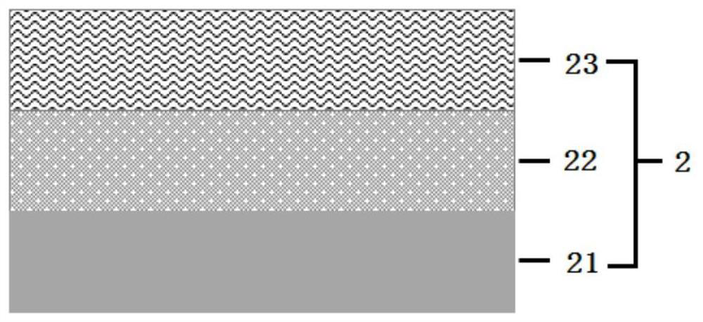
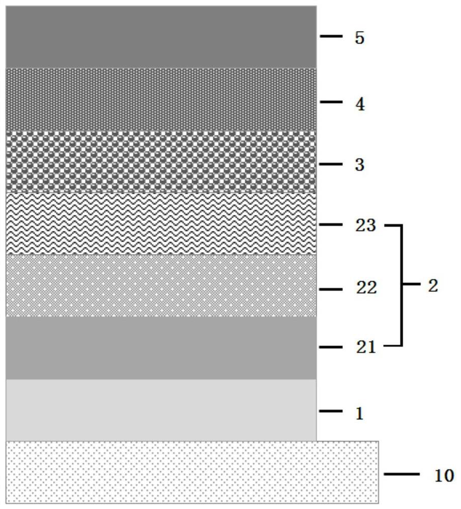
[0039] An interfacial layer is prepared between the hole transport layer and the hole injection layer, wherein the hole injection layer is disposed adjacent to the anode, and the material of the hole injection layer contains a transition metal oxide; the hole transport The layer is arranged adjacent to the quantum dot light-emitting layer, and the material of the hole transport layer contains organic hole transport material; the material of the interface layer is a graphene material.
[0040] The preparation method of the quantum dot light-emitting diode provided by the embodiment of the present invention can be realized only by preparing an interface layer between the hole transport layer and the hole injection layer on the basis of the conventional quantum dot light-emitting diode preparat...
Embodiment 1
[0049] A method for preparing a quantum dot light-emitting diode, comprising the following steps:
[0050] Using transparent conductive film ITO as the anode, the thickness of the anode is 50nm;
[0051] Deposition of WO on the anode by solution processing 3 Nanoparticles, annealed at 100°C for 30 minutes to prepare a hole injection layer, the thickness of the hole injection layer is 30nm;
[0052] Depositing reduced graphene oxide on the hole injection layer by solution processing method, and annealing at 70°C for 30 minutes to prepare an interface layer, the thickness of the interface layer is 5nm;
[0053] Depositing PVK on the interface layer by a solution processing method, and annealing at 150°C for 30 minutes to prepare an organic hole transport layer, the thickness of the organic hole transport layer is 20nm;
[0054] Depositing CdSe / ZnS on the organic hole transport layer by a solution processing method, and annealing at 100°C for 30 minutes to prepare a quantum dot...
Embodiment 2
[0058] A method for preparing a quantum dot light-emitting diode, comprising the following steps:
[0059] Using transparent conductive film ITO as the anode, the thickness of the anode is 50nm;
[0060] Deposition of V on the anode by solution processing2 o 5 Nanoparticles, annealed at 100°C for 30 minutes to prepare a hole injection layer, the thickness of the hole injection layer is 30nm;
[0061] Depositing graphene oxide on the hole injection layer by a solution processing method, annealing at 180° C. for 60 minutes to prepare an interface layer, the thickness of the interface layer is 3 nm;
[0062] Depositing PVK on the interface layer by solution processing method, annealing at 150° C. for 30 minutes to prepare an organic hole transport layer, the thickness of the organic hole transport layer is 20 nm;
[0063] Depositing CdSe / ZnS on the organic hole transport layer by a solution processing method, and annealing at 100°C for 30 minutes to prepare a quantum dot lumine...
PUM
| Property | Measurement | Unit |
|---|---|---|
| thickness | aaaaa | aaaaa |
| thickness | aaaaa | aaaaa |
| thickness | aaaaa | aaaaa |
Abstract
Description
Claims
Application Information
 - R&D
- Intellectual Property
- Life Sciences
- Materials
- Tech Scout
- Unparalleled Data Quality
- Higher Quality Content
- 60% Fewer Hallucinations
Browse by: Latest US Patents, China's latest patents, Technical Efficacy Thesaurus, Application Domain, Technology Topic, Popular Technical Reports.
© 2025 PatSnap. All rights reserved.Legal|Privacy policy|Modern Slavery Act Transparency Statement|Sitemap|About US| Contact US: help@patsnap.com