Addressing method and module applied to on-chip control system and on-chip control system

An on-chip control and addressing module technology, applied in memory systems, memory address/allocation/relocation, instruments, etc., can solve problems such as information flow access bottlenecks, improve addressing efficiency and stability, and have high management flexibility Effect

Inactive Publication Date: 2020-07-10
宁波中控微电子有限公司
View PDF5 Cites 5 Cited by
  • Summary
  • Abstract
  • Description
  • Claims
  • Application Information

AI Technical Summary

Problems solved by technology

[0007] The present invention provides an addressing method, a module and an on-chip control system applied to an on-chip control system in order to solve the problem that the above-mentioned Von Neumann structure may cause a bottleneck in the information flow access of the CPU and the control program processor to the memory

Method used


Image

  • Addressing method and module applied to on-chip control system and on-chip control system
  • Addressing method and module applied to on-chip control system and on-chip control system
  • Addressing method and module applied to on-chip control system and on-chip control system

Examples


Embodiment 1

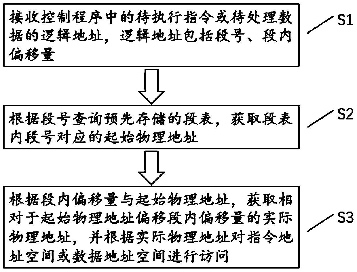
[0049] see figure 1 , the application provides an addressing method applied to an on-chip control system. The on-chip control system includes a central processing unit, a control program processor, and a memory. The central processing unit directly addresses the memory through a real physical address, and part of the address space of the memory It is configured to store the instruction address space of the instruction segment and the data address space of the data segment, and control the program processor to address the instruction address space or the data address space through the address translation of the logical address, including the following steps:

[0050] S1: Receive the logical address of the instruction to be executed or the data to be processed in the control program. The logical address includes the segment number and the offset within the segment;

[0051] S2: Query the pre-stored segment table according to the segment number, and obtain the starting physical a...

Embodiment 2

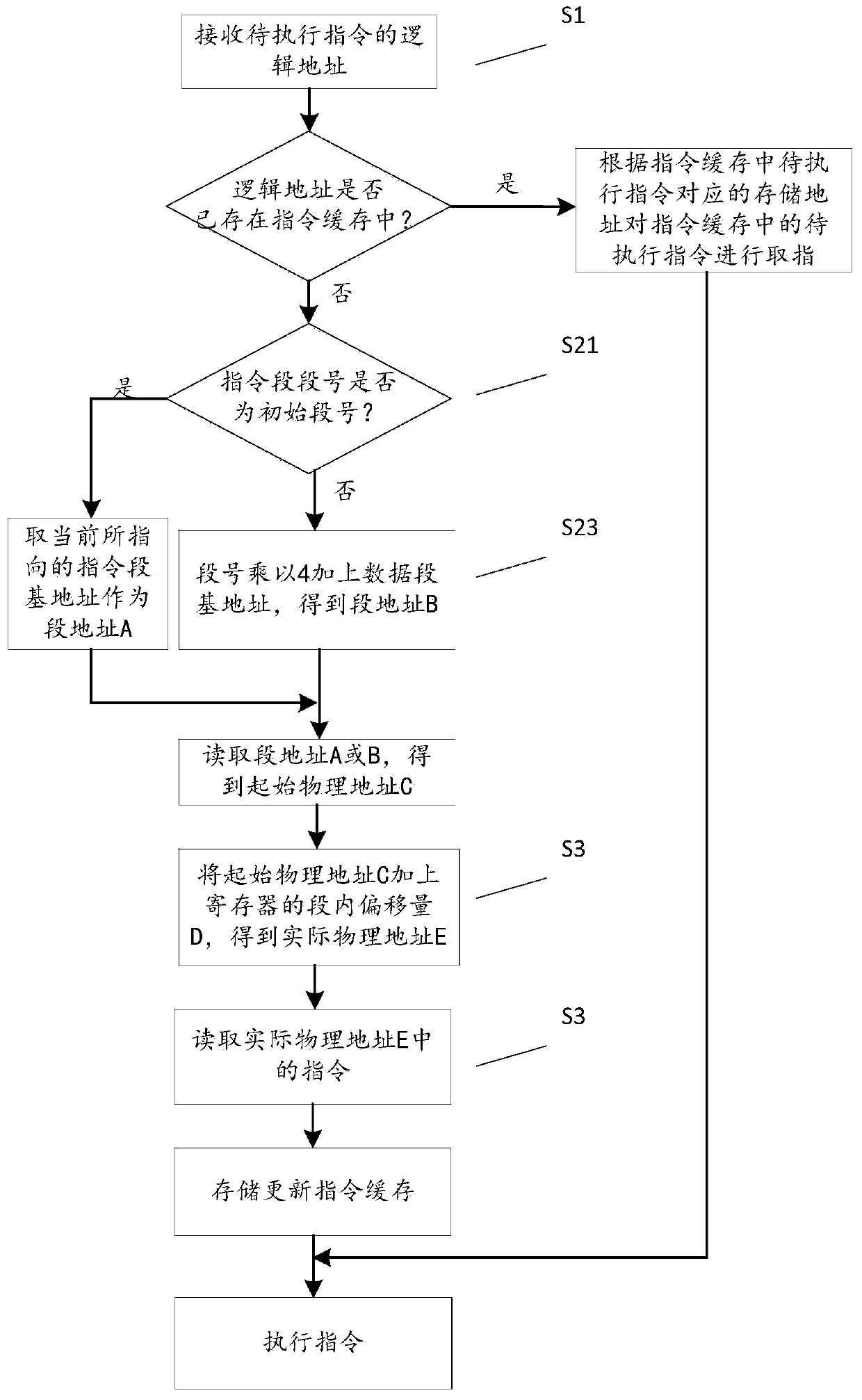
[0068] see Figure 6 , the present application provides an addressing module 100 applied to an on-chip control system based on Embodiment 1. The control program processor applied to the on-chip control system addresses the instruction address space or data address space of the memory, including:

[0069] The receiving sub-module 101 is used to receive the logical address of the instruction to be executed or the data to be processed in the control program, and the logical address includes a segment number and an offset within the segment;

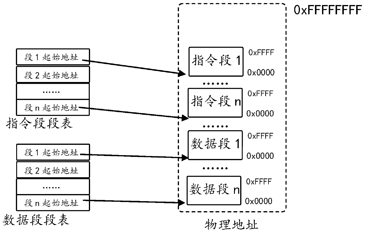
[0070] Address conversion sub-module 102, address conversion sub-module 102 is pre-stored with a segment table storing the initial physical addresses of each instruction segment and data segment, address conversion sub-module 102 is used to query the segment table according to the segment number, and obtain the segment number in the segment table The corresponding starting physical address, and according to the offset in the segment and the ...

Embodiment 3

[0083] see Figure 7 and Figure 8 , the present application provides an on-chip control system, including a central processing unit 1, a control program processor 2, a memory 3, and an addressing module 100 based on Embodiment 2, wherein the addressing module 100 is located in the control program processor 2 (eg Figure 7 shown) or hang on the on-chip bus 4 of the on-chip control system as an independent IP core (such as Figure 8 As shown), the central processing unit 1 directly addresses the memory 3 based on the real physical address, and the control program processor 2 addresses the instruction address space or the data address space of the memory 3 through the addressing module 100 based on the logical address.

[0084] see Figure 7 In this embodiment, the addressing module 100 is set in the control program processor as an example to describe this embodiment in detail, but it is not limited thereto.

[0085] The addressing module of this embodiment is connected to t...


PUM


Abstract

The invention discloses an addressing method and module applied to an on-chip control system and the on-chip control system. The on-chip control system comprises a central processing unit, a control program processor and a memory; the central processing unit directly addresses the memory through the real physical address; the control program processor addresses an instruction address space or a data address space of the memory through address conversion of a logic address, and the addressing method comprises the following steps: S1, receiving the logic address of a to-be-executed instruction or to-be-processed data in a control program, wherein the logic address comprises a segment number and an in-segment offset; S2, querying a pre-stored segment table according to the segment number, andobtaining an initial physical address; S3, acquiring an actual physical address according to the intra-segment offset and the initial physical address, and accessing the memory according to the actual physical address. According to the method, the problem that a von Neumann structure may cause information flow access bottlenecks of a CPU and a control program processor to a memory is solved, andthe addressing efficiency and stability of the system are improved.

Description

technical field [0001] The invention belongs to the technical field of on-chip control systems, and in particular relates to an addressing method, a module and an on-chip control system applied to the on-chip control system. Background technique [0002] The storage structure of the current system-on-chip (SoC) is usually divided into a von Neumann structure and a Harvard structure. [0003] The von Neumann architecture, also known as the Princeton architecture, is a memory structure that combines program instruction memory and data memory. Program instruction storage addresses and data storage addresses point to different physical locations in the same memory, so program instructions and data have the same width. Von Neumann defined three basic principles of computer manufacturing, namely, the use of binary logic, program storage and execution, and the computer is composed of five parts (calculator, controller, memory, input device, output device). [0004] In order to av...

Claims


Application Information

Patent Timeline
Patent Type & Authority Applications(China)
IPC IPC(8): G06F12/06G06F12/0831
CPCG06F12/0653G06F12/0831
Inventor 杨大胜唐艳丽来晓郑慧娴何超曹焱
Owner 宁波中控微电子有限公司
Why Eureka
Try Eureka