

Array type multistage semiconductor refrigeration method for large-target-surface detector
A detector array and semiconductor technology, applied in the direction of semiconductor devices, electric solid devices, radiation control devices, etc., can solve the problems of large volume, affecting the cooling effect of detectors, complex structure, etc., to improve efficiency, suppress dark current noise, Effect of reducing thermal resistance
- Summary
- Abstract
- Description
- Claims
- Application Information
AI Technical Summary
Problems solved by technology
Method used
Image

Examples
specific Embodiment approach 1
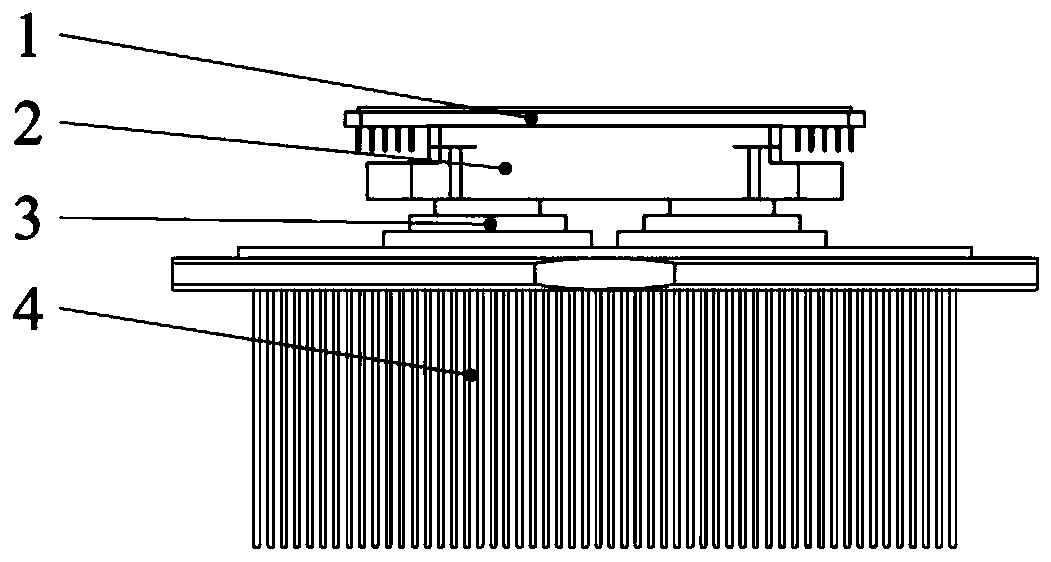
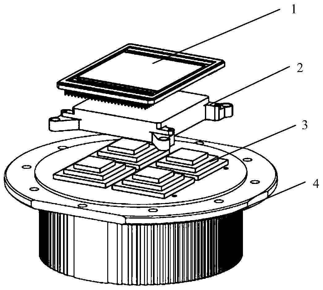
[0013] Specific implementation mode 1. Combination figure 1 and figure 2 Describe this embodiment, a large target surface (pixel 6K × 6K) detector array multi-stage semiconductor refrigeration device, including a large target surface (pixel 6K × 6K) detector 1, cold plate 2, array multistage semiconductor refrigerator 3 and heat sink 4, using a 2×2 array of multi-stage semiconductor coolers to cool the large target surface (pixel 6K×6K) detectors, using series, parallel or series-parallel combinations between the semiconductor coolers, the array Low-temperature solder is used for welding between the hot end and the heat sink of the semiconductor refrigerator, and between the cold end of the array semiconductor and the cold plate. The low-temperature solder refers to the solder with a melting point of <200°C. The molten low-temperature solder can form a metallographic structure at the weld after cooling , so that there is no gap between the semiconductor cooler and the cold p...
PUM
 Abstract
Description
Claims
Application Information