Supercharge Your Innovation With Domain-Expert AI Agents!

Silicon wafer surface defect visual detection device and detection method

A visual inspection device and a technology for the surface of silicon wafers, which are used in measurement devices, optical testing of flaws/defects, and material analysis by optical means. It can solve problems such as inability to obtain silicon wafers accurately, reduce manual intervention, and improve the success rate. and efficiency, the effect of high practical value

Inactive Publication Date: 2020-07-17
TIANJIN UNIV
View PDF7 Cites 11 Cited by
  • Summary
  • Abstract
  • Description
  • Claims
  • Application Information

AI Technical Summary

Problems solved by technology

This method generally cannot accurately obtain complete silicon wafer surface defects

Method used


Image

  • Silicon wafer surface defect visual detection device and detection method
  • Silicon wafer surface defect visual detection device and detection method
  • Silicon wafer surface defect visual detection device and detection method

Examples


Embodiment Construction

[0065] A silicon wafer surface defect visual detection device and detection method of the present invention will be described in detail below in conjunction with the embodiments and the accompanying drawings.

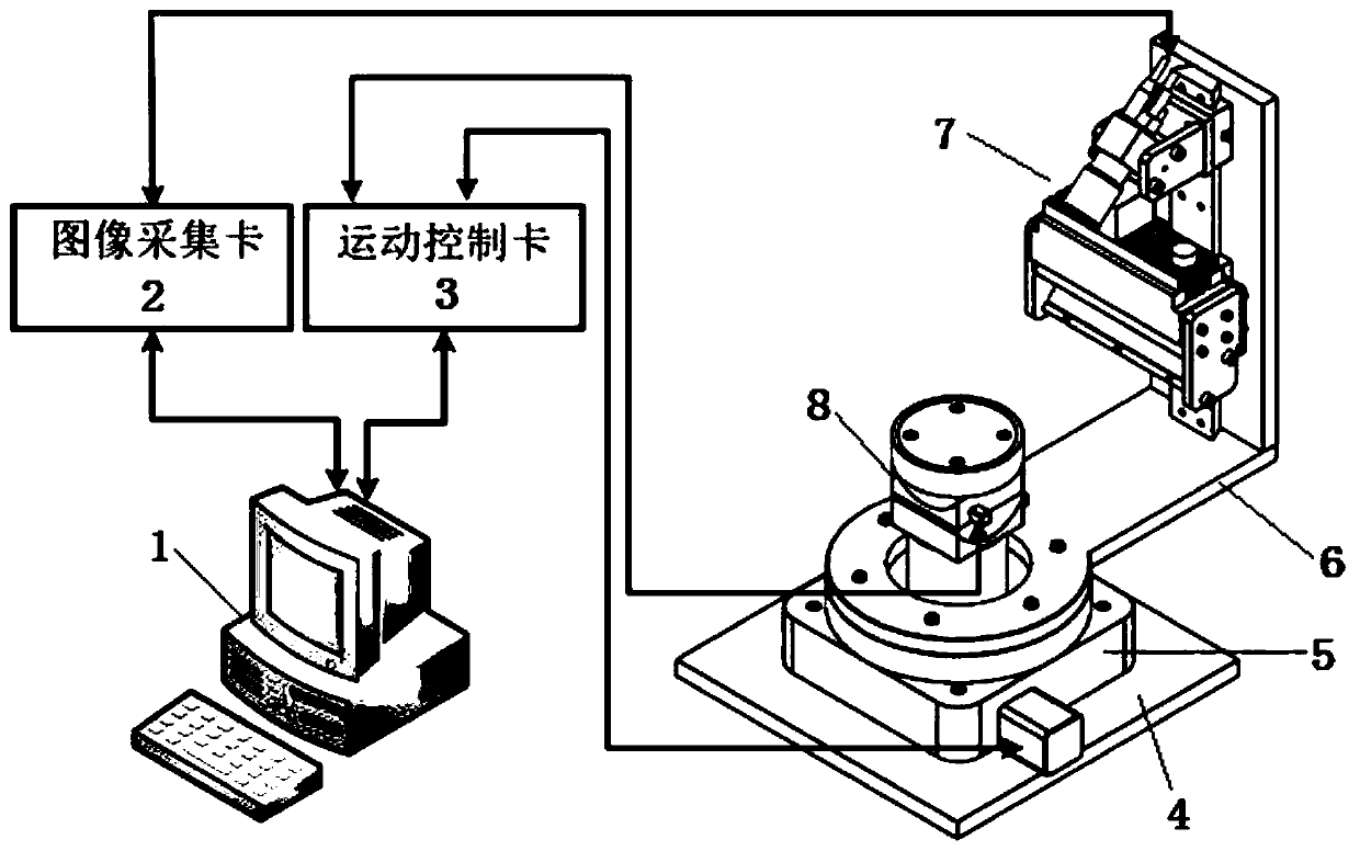
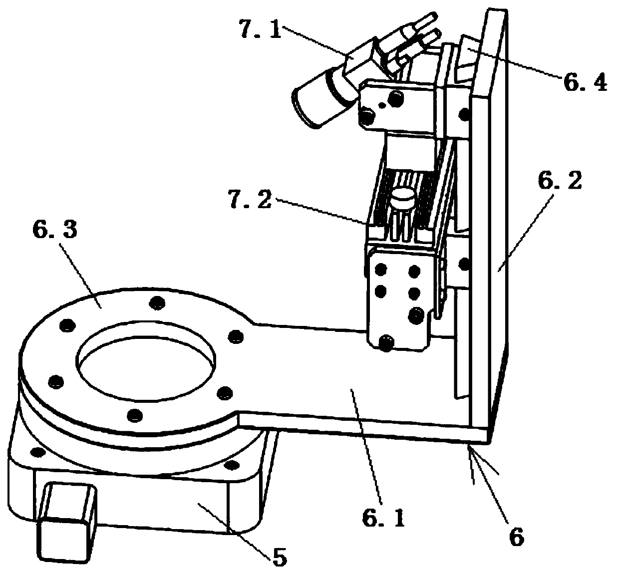
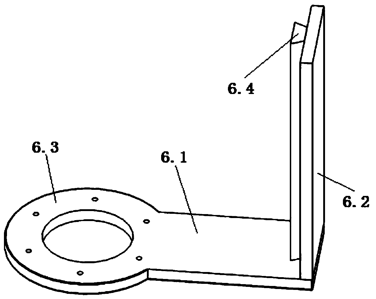
[0066] Such as figure 1 As shown, a visual detection device for silicon wafer surface defects of the present invention includes a computer 1, an image acquisition card 2 and a motion control card 3 connected to the computer 1 respectively, and the image acquisition part of the computer 1 passes through the image acquisition card 2 Connect the lighting and imaging unit 7, the drive control part of the computer 1 is respectively connected to the silicon wafer carrier 8 and the hollow electric rotary table 5 through the motion control card 3, wherein the hollow electric rotary table 5 is fixed on the machine platform 4 , and connect the illumination imaging unit 7 through the L-shaped connection bracket 6 fixed on the hollow electric rotary table 5, for driving the illumin...


PUM


Abstract

The invention discloses a silicon wafer surface defect visual detection device and detection method; the device has the image acquisition card and the motion control card that are respectively connected with the computer; an image acquisition part of the computer is connected with the illumination imaging unit through an image acquisition card; a driving control part of the computer is respectively connected with the silicon wafer bearing platform and the hollow electric rotating platform through a motion control card; the hollow electric rotary table is fixed on the machine table, and connected with the illumination imaging unit through an L-shaped connecting bracket fixed on the hollow electric rotary table; the illumination imaging unit is driven to rotate by taking the central axis ofthe silicon wafer bearing platform as an axis under the control of the computer; the bottom end of the silicon wafer bearing platform sequentially penetrates through the front end of the horizontal part of the L-shaped connecting bracket and a center through hole of the hollow electric rotary table to be fixed to the machine table; the silicon wafer bearing platform is connected with the motion control card, and therefore the silicon wafer to be detected is driven to be finely adjusted under the control of the computer to reach the optimal image taking position. According to the invention, the silicon wafer defect image acquisition speed is effectively improved, and the silicon wafer detection success rate and efficiency are effectively improved.

Description

technical field [0001] The invention relates to the detection of surface defects of a silicon wafer. In particular, it relates to a silicon wafer surface defect visual detection device and detection method for synchronous image acquisition based on a rotating illumination light source and a camera. Background technique [0002] Silicon wafer is an important upstream product for making solar cells and semiconductor devices, and its quality seriously affects the production and work efficiency of subsequent products. In the automatic production process of silicon wafers, the quality inspection of surface defects is an important part. The surface defects of silicon wafers can be divided into holes, chipping, stains, scratches, etc. At present, in most silicon wafer manufacturing enterprises, the quality monitoring of silicon wafers mainly relies on manual visual inspection, which has the advantages of high work intensity, low efficiency, and inspection. Low yield and secondary...

Claims


Application Information

Patent Timeline
Patent Type & Authority Applications(China)
IPC IPC(8): G01N21/88G01N21/95
CPCG01N21/8806G01N21/95G01N2021/8841
Inventor 田庆国肖舒琦段语嫣高小婷周万欣
Owner TIANJIN UNIV
Features
  • R&D
  • Intellectual Property
  • Life Sciences
  • Materials
  • Tech Scout
  • Unparalleled Data Quality
  • Higher Quality Content
  • 60% Fewer Hallucinations
Learn More