

PCB and PIN crimping device and use method thereof
A technology of PCB board and needle pressing, applied in the structural connection of printed circuits, multi-layer circuit manufacturing, printed circuit components, etc., can solve the problems of increased manufacturing costs, component damage, low transmission speed, etc., and achieve the reduction of complex requirements , Improve production efficiency and reduce manufacturing costs
- Summary
- Abstract
- Description
- Claims
- Application Information
AI Technical Summary
Problems solved by technology
Method used
Image

Examples
Embodiment 1
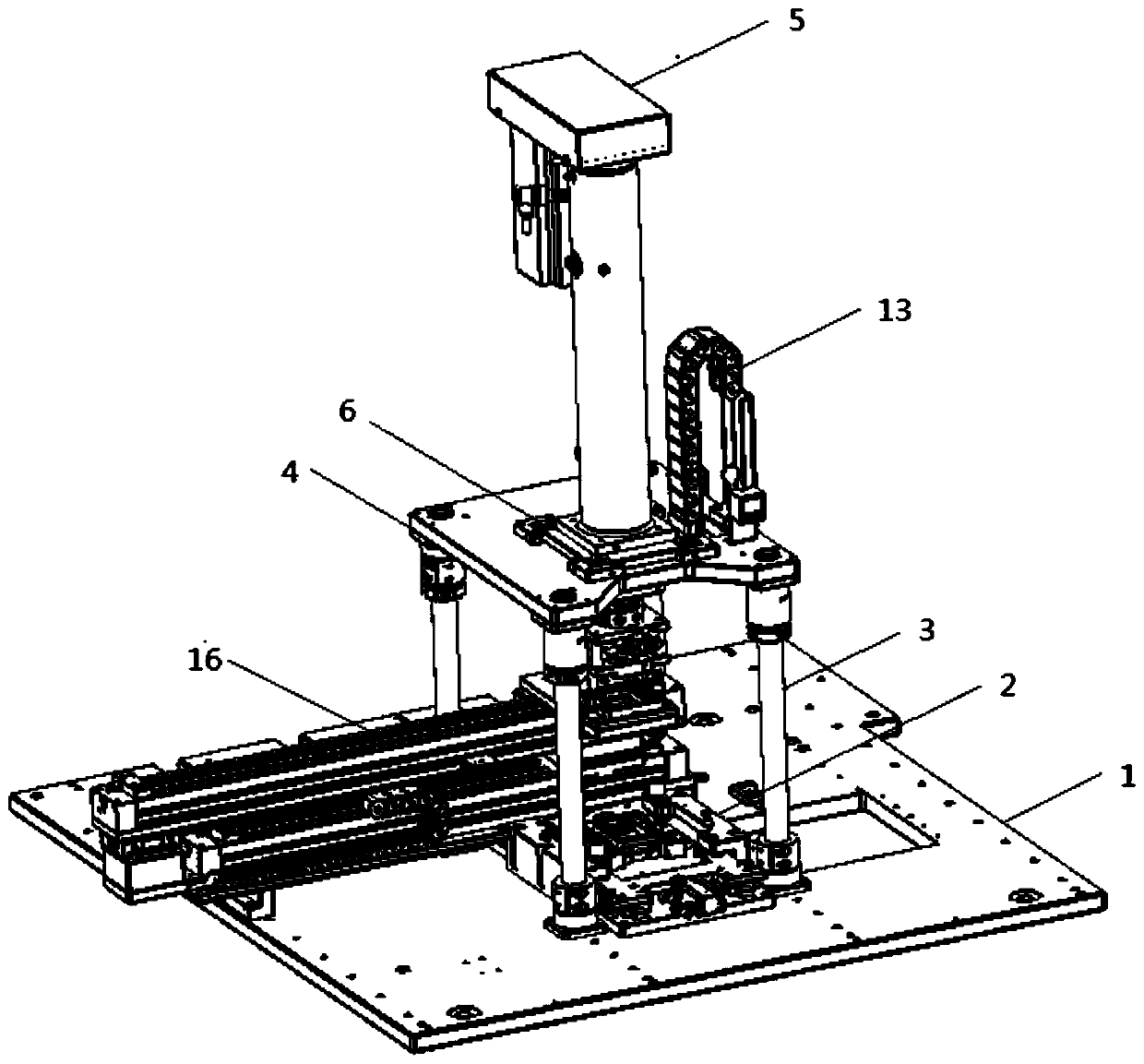
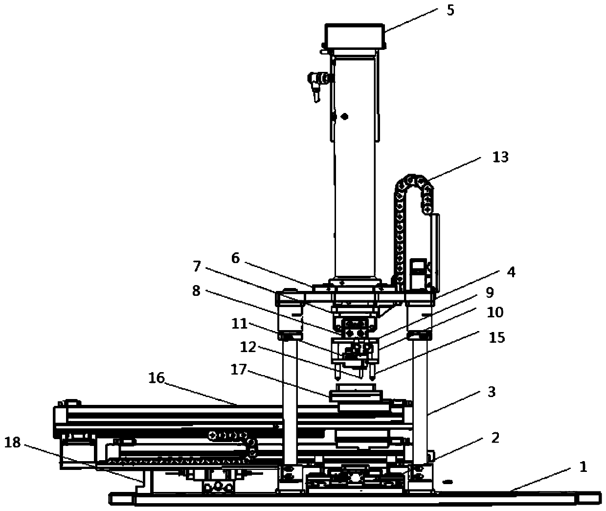
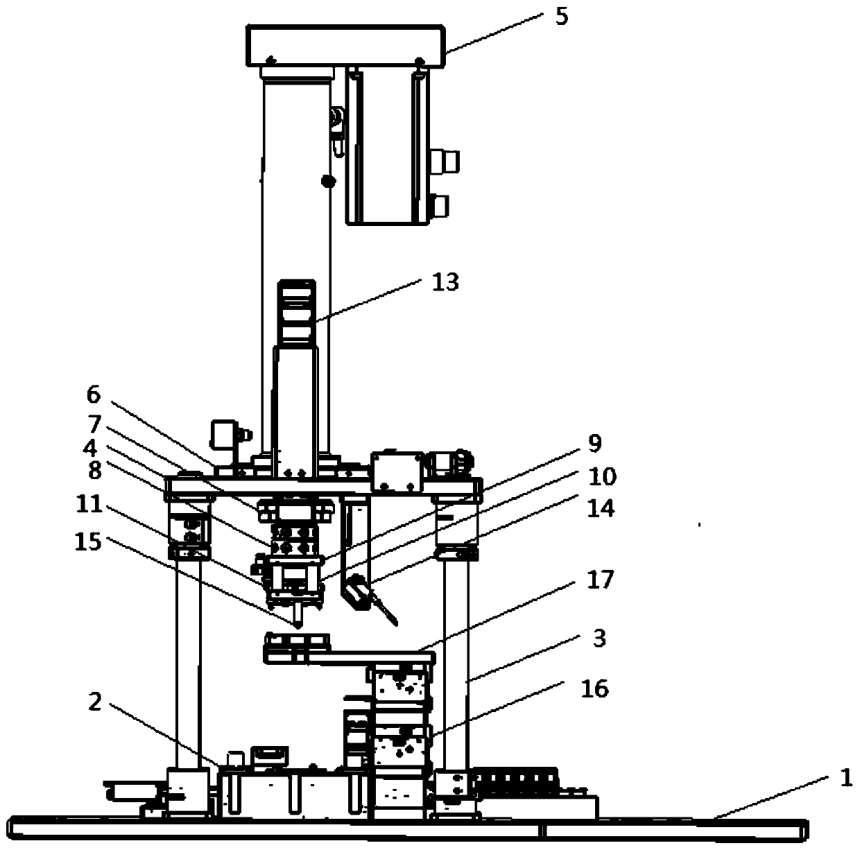
[0050] This embodiment mainly introduces the basic composition and connection relationship of a PCB board and PIN needle crimping device of the present invention.
[0051] like figure 1 As shown in , it shows a perspective view of a PCB board and PIN pin crimping device; figure 2 As shown, it shows a front view of a PCB board and PIN pin crimping device; as image 3 As shown in , it shows a left side view of a PCB board and PIN pin crimping device, such as Figure 4 As shown, it shows a top view of a PCB board and PIN pin crimping device.
[0052] to combine figure 1 , 2 As shown in , 3 and 4, a PCB board and PIN pin crimping device provided in the embodiment of the present application, the device includes a support unit, a power unit and a transmission unit, and the structure of the support unit is a bracket with a base 1 , used to carry the power unit and the transmission unit, the power unit and the transmission unit are located on the bracket, the power unit is conne...
Embodiment 2
[0069] On the basis of Embodiment 1, this embodiment further proposes a method for using a PCB board and PIN pin crimping device, and the same technical features and technical descriptions as Embodiment 1 will not be repeated in this embodiment.
[0070] combine Figure 1~6 As shown, the method of using the PCB board and the PIN pin crimping device is as follows:
[0071] Step 1: Preliminary positioning is achieved by controlling the screw in and out of the adjustment screw on the press adjustment plate 6, and adjust the position of the servo press 5 in the horizontal direction, the purpose of which is to make the PCB board clamp the module and set it below it The axis of symmetry of the pallet 2 in the vertical direction basically coincides;
[0072] Step 2: The pneumatic module 16 transferred by the PCB carrier is connected to the cylinder (not shown in the figure) through the air pipe, the solenoid valve 19 sends a signal to control the communication of the air circuit, an...
PUM
 Abstract
Description
Claims
Application Information