Bismuth selenide oxide nanosheet photoelectric detector treated by oxygen plasma and preparation method

An oxygen plasma and photodetector technology, applied in semiconductor devices, circuits, electrical components, etc., can solve the problems of low carrier mobility, limited application range, non-uniform material properties, and low responsivity, etc. The effect of popularization and application, low cost and high switching ratio

Inactive Publication Date: 2020-07-28
HUAZHONG UNIV OF SCI & TECH
View PDF3 Cites 4 Cited by
  • Summary
  • Abstract
  • Description
  • Claims
  • Application Information

AI Technical Summary

Problems solved by technology

Two-dimensional photodetectors have many advantages. For example, graphene detectors have a wide range of spectral detection and ultra-fast response. However, graphene has little responsivity to light due to its zero band gap and low light absorption coefficient in applications. Transparency, flexibility, easy handling, and adjustable bandgap of transition metal chalcogenides make transition metal chalcogenide photodetectors flexible and detect different light wavelengths, but the low carrier mobility limits the scope of appl

Method used


Image

  • Bismuth selenide oxide nanosheet photoelectric detector treated by oxygen plasma and preparation method
  • Bismuth selenide oxide nanosheet photoelectric detector treated by oxygen plasma and preparation method
  • Bismuth selenide oxide nanosheet photoelectric detector treated by oxygen plasma and preparation method

Examples


preparation example Construction

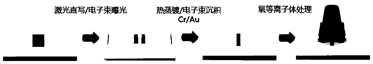
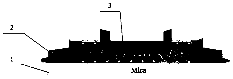
[0030] see figure 1 and figure 2 , the preparation method of the bismuth selenium oxide nanosheet photodetector that the oxygen plasma treatment provided by the present invention mainly comprises the following steps:

[0031] Step 1, preparing bismuth selenium oxide nanosheets on the substrate by chemical vapor deposition.

[0032] In this embodiment, the substrate is an insulating material, which is a mica sheet; the thickness of the bismuth selenium oxide nanosheet is 10nm-100nm, and its shape is a square.

[0033] Step 2, using laser direct writing or electron beam exposure technology, combined with thermal evaporation and electron beam evaporation technology to prepare a pair of source-drain metal electrodes on the bismuth selenium oxide nanosheet.

[0034] In this embodiment, the source-drain metal electrode is a chromium-gold composite electrode, wherein the thickness of chromium is 5nm-10nm, and the thickness of gold is 50nm-100nm.

[0035] Specifically, a metal ele...


PUM

PropertyMeasurementUnit
Thicknessaaaaaaaaaa
Thicknessaaaaaaaaaa
Thicknessaaaaaaaaaa

Abstract

The invention belongs to the related technical field of photoelectric detection and discloses an oxygen plasma treated bismuth oxyselenide nanosheet photoelectric detector and a preparation method. The preparation method comprises the following steps of (1) preparing a bismuth oxyselenide nanosheet on a substrate by using a chemical vapor deposition method; (2) preparing a pair of source-drain metal electrodes on the bismuth oxyselenide nanosheet by adopting a laser direct writing or electron beam exposure technology in combination with thermal evaporation and electron beam evaporation; and (3) carrying out oxygen plasma treatment of the bismuth oxyselenide nanosheet to obtain a bismuth oxyselenide nanosheet photoelectric detector. The preparation method is advantaged in that a plasma processing method is adopted, the preparation method is simple in process, easy to operate and relatively low in cost, is expected to be applied to large-scale improvement of performance of a bismuth oxyselenide nanosheet photoelectric detector, and lays a foundation for application of bismuth oxyselenide in the photoelectric detector.

Description

technical field [0001] The invention belongs to the technical field related to photoelectric detection, and more specifically relates to a bismuth selenium oxide nanosheet photodetector processed by oxygen plasma and a preparation method thereof. Background technique [0002] The conversion technology of photoelectric signals has greatly affected daily life and has a wide range of applications, including visual imaging, optical communication, gas phase sensing and detectors, etc. Although the size and application range of photoelectric detection platforms are gradually expanding, the speed, In terms of efficiency, wavelength range, flexibility, transparency, and compatibility, there is an increasing demand for higher-performance photodetection. [0003] Two-dimensional materials represented by graphene have many excellent electrical, optical, mechanical and thermal properties, especially in terms of photoelectric properties. Two-dimensional materials are likely to replace tr...

Claims


Application Information

Patent Timeline
IPC IPC(8): H01L31/0216H01L31/101H01L31/18H01L31/032
CPCH01L31/02161H01L31/032H01L31/101H01L31/186H01L31/1876Y02P70/50
Inventor 诸葛福伟熊绪婧翟天佑
Owner HUAZHONG UNIV OF SCI & TECH
Why Eureka
Try Eureka