Display panel and manufacturing method thereof, and display device

A display panel and substrate technology, which is applied in the direction of instruments, character and pattern recognition, electrical components, etc., can solve problems such as high cost, unfavorable thinning of display panels, complex display panel technology, etc., to reduce production costs and improve fingerprint recognition accuracy , The effect of simplifying the production process

Active Publication Date: 2020-07-31
HEFEI VISIONOX TECH CO LTD
View PDF4 Cites 9 Cited by
  • Summary
  • Abstract
  • Description
  • Claims
  • Application Information

AI Technical Summary

Problems solved by technology

[0004] However, the existing display panel including the opening of a light-shielding film layer with small holes is relatively complex and costly, and is not conducive to the thinning of the display panel.

Method used


Image

  • Display panel and manufacturing method thereof, and display device
  • Display panel and manufacturing method thereof, and display device
  • Display panel and manufacturing method thereof, and display device

Examples


Embodiment Construction

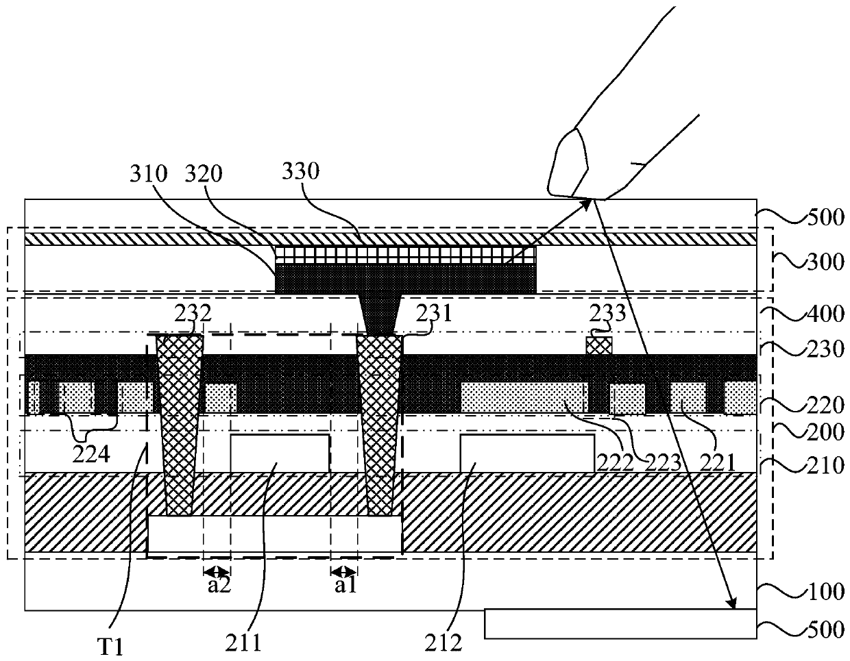
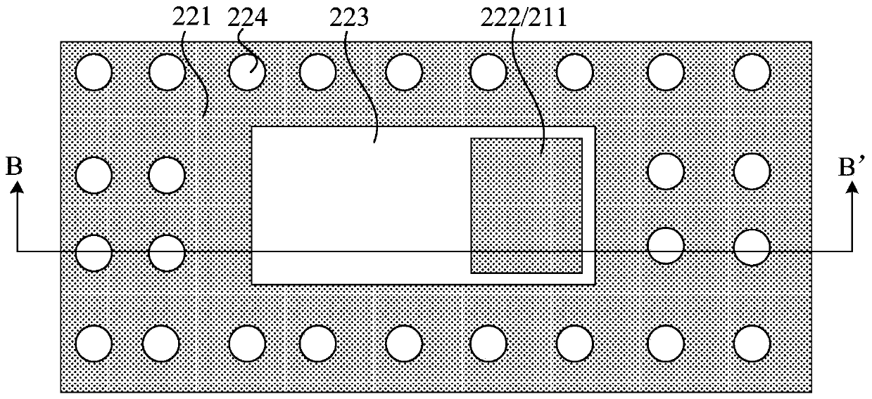
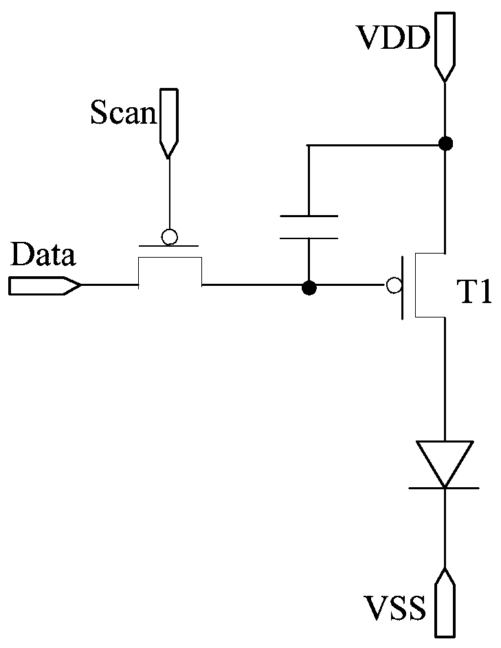
[0044] The present invention will be further described in detail below in conjunction with the accompanying drawings and embodiments. It should be understood that the specific embodiments described here are only used to explain the present invention, but not to limit the present invention. In addition, it should be noted that, for the convenience of description, only some structures related to the present invention are shown in the drawings but not all structures.

[0045] As mentioned in the background art, the existing display panel including the light-shielding film layer with small holes is relatively complex in process and high in cost, and is not conducive to the thinning of the display panel. The inventors have found through research that the reason for the above problems is that in the existing display panels that include a light-shielding film layer with small holes, an additional light-shielding film layer is usually added on the basis of the film layer structure of ...


PUM


Abstract

The embodiment of the invention discloses a display panel and a manufacturing method thereof, and a display device. According to the display panel, an array circuit layer in the display panel comprises at least three metal layers arranged on one side of a substrate; the metal layer comprises a circuit structure part; any one of the at least three metal layers is used as a light shading layer; at least one of the other metal layers is used as an auxiliary light shading layer; the light shading layer comprises a light shading part; the light shading part and the circuit structure part on the same layer are arranged in an insulating manner to form a hollow part; the light shading part is provided with at least one via hole; and the via hole is not overlapped with the auxiliary light shading layer and a first electrode layer in the thickness direction of the display panel; and the orthogonal projection of the first electrode layer and / or the auxiliary light shading layer on the substrate covers the orthogonal projection of the hollow part on the substrate. According to the technical scheme, the manufacturing process of the display panel can be simplified, the production cost can be reduced, lightening and thinning of the display panel are facilitated, and improvement of fingerprint identification precision is facilitated.

Description

technical field [0001] Embodiments of the present invention relate to the field of display technologies, and in particular, to a display panel, a manufacturing method thereof, and a display device. Background technique [0002] With the development of display technology, under-display fingerprint recognition structures are more and more widely used in display panels. [0003] In the existing display panel, the optical fingerprint recognition technology developed by using the principle of pinhole imaging is widely used due to its high precision. image sensing system, matrix pinhole imaging system) layer. [0004] However, the existing display panel including the light-shielding film layer with small holes is relatively complicated in technology and high in cost, and is not conducive to the thinning of the display panel. Contents of the invention [0005] The invention provides a display panel, a manufacturing method thereof, and a display device, so as to realize fingerpr...

Claims


Application Information

Patent Timeline
Patent Type & Authority Applications(China)
IPC IPC(8): H01L27/12H01L27/32G06K9/00
CPCH01L27/124G06V40/1324H10K59/40H10K59/126H10K59/131
Inventor 蔡俊飞
Owner HEFEI VISIONOX TECH CO LTD
Why Eureka
Try Eureka