PCB component automatic detection and assembling device and method

An automatic detection and assembly device technology, which is applied in the direction of measuring devices, devices for coating liquid on the surface, measuring electricity, etc., can solve problems such as insufficient locking, material supply blockage or broken material, waste of time and cost, etc., and achieve reduction Manual participation, uniform glue application, and the effect of avoiding misapplication

Active Publication Date: 2020-08-04
西安精雕精密机械工程有限公司
View PDF8 Cites 7 Cited by
  • Summary
  • Abstract
  • Description
  • Claims
  • Application Information

AI Technical Summary

Problems solved by technology

[0029] Although this solution saves the steps of manual material preparation, taking and putting in finished materials, and the operation process is relatively simplified, it still needs to manually take and lock screws. Repeated mechanical operations for a long time will easily make people tired, resulting in missing locks, Locking is not in place and other operational errors; on the other hand, the conveyor body of this assembly line is generally running all the time, which has strict requirements on the beat of each station on the production line. If the beat is not suitable, It is prone to material supply blockage or material breakage, personnel waiting for material, waste of time and cost

Method used


Image

  • PCB component automatic detection and assembling device and method
  • PCB component automatic detection and assembling device and method
  • PCB component automatic detection and assembling device and method

Examples


Embodiment Construction

[0093] In describing the present invention, it should be understood that the terms "center", "longitudinal", "transverse", "upper", "lower", "front", "rear", "left", "right", " The orientation or positional relationship indicated by "vertical", "horizontal", "top", "bottom", "inner", "outer", "side", "end", "side" etc. is based on the Orientation or positional relationship is only for the convenience of describing the present invention and simplifying the description, and does not indicate or imply that the referred device or element must have a specific orientation, be constructed and operated in a specific orientation, and thus should not be construed as a limitation of the present invention. In addition, the terms "first" and "second" are used for descriptive purposes only, and cannot be interpreted as indicating or implying relative importance or implicitly specifying the quantity of indicated technical features. Thus, a feature defined as "first" and "second" may explicit...


PUM


Abstract

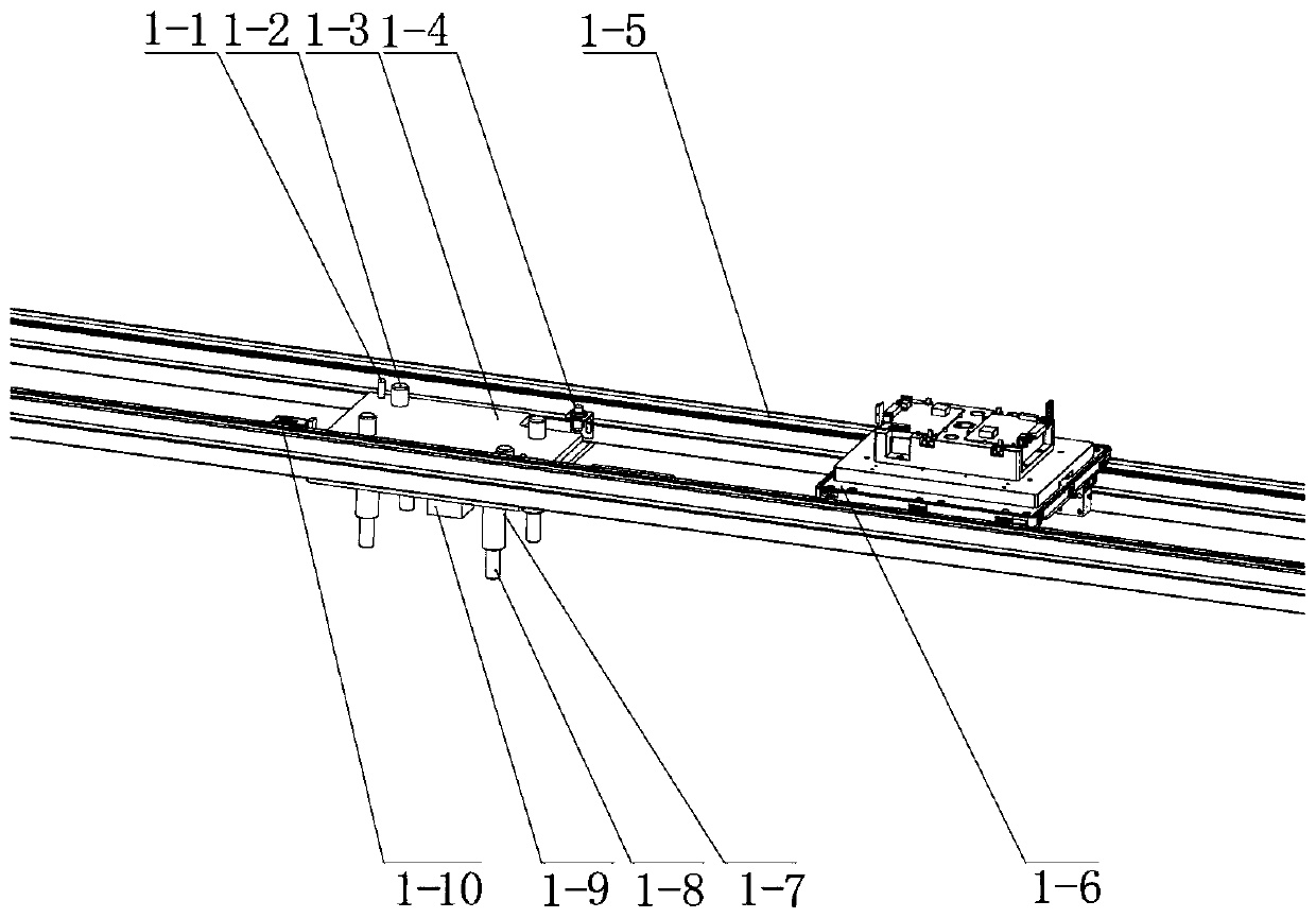
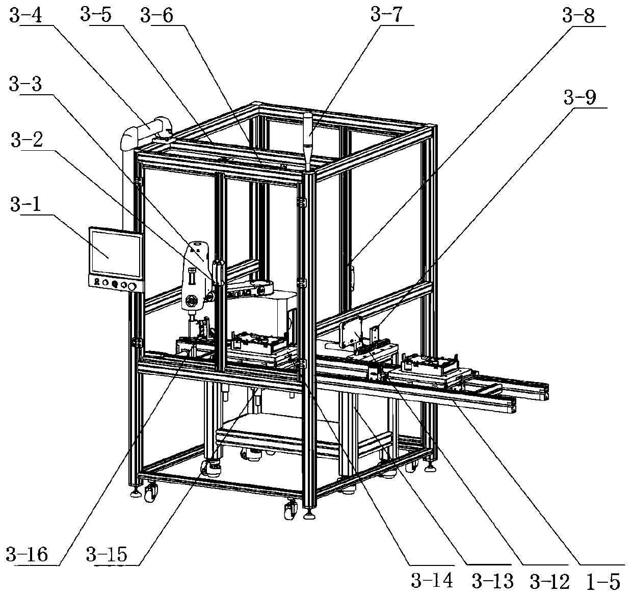
The invention discloses a PCB component automatic detection and assembling device and method. According to the PCB component automatic detection and assembling device and method, a PCB component automatic detection device, a PCB component automatic gluing device and a PCB component automatic screw-locking device are sequentially arranged on a basic line body unit, a pneumatic stopper, a secondarylocating mechanism and a tray-and-tool are sequentially arranged on an assembly line body, locating pins and locating columns are arranged at one side, close to the pneumatic stopper, of the upper portion of the secondary locating mechanism, a guide shaft is arranged at the lower end of each locating column, and a linear bearing is arranged in each guide shaft; and a proximity switch is arranged at one side close to the tray-and-tool, an air cylinder is arranged on the lower portion of the secondary locating mechanism, and the PCB component automatic detection device, the PCB component automatic gluing device and the PCB component automatic screw-locking device are connected with an industrial personal computer respectively and are used for realizing automatic detection, gluing and screw-locking operation on a PCB component. Through the PCB component automatic detection and assembling device and method, the automatic degree is high in the whole detection process, manpower is saved, efficiency is high, an error cannot be easily made, detection reliability is high, and replacement of a man with a machine is completely realized.

Description

technical field [0001] The invention belongs to the technical field, and in particular relates to a PCB assembly automatic detection and assembly device and a method thereof. Background technique [0002] At present, in the process of assembling PCB circuit boards into finished products in the electronic assembly industry, multiple inspection and assembly processes need to be completed. Take the servo drive in the industrial control field as an example, such as the inspection of PCB components (including power supply test, parameter read and write, and drive test. etc.), gluing components on PCB components, screw locking during component assembly, etc. These tasks are mainly completed by manual operations. [0003] With the advancement of science and technology, more and more electronic products are developing in the direction of miniaturization and intelligence. Most smart electronic products are composed of various PCB circuit boards, including power boards, control board...

Claims


Application Information

Patent Timeline
Patent Type & Authority Applications(China)
IPC IPC(8): B23P19/06G01R31/28B05C5/02B05C13/02B05C11/10B05D1/26
CPCB23P19/06G01R31/2806B05C5/0208B05C13/02B05C11/1002B05D1/26
Inventor 梁传秋高创平庆伟
Owner 西安精雕精密机械工程有限公司
Why Eureka
Try Eureka