Semiconductor process chamber, wafer edge protection method and semiconductor equipment

A process chamber and edge protection technology, applied in discharge tubes, electrical components, circuits, etc., can solve the problems of edge protection ring failure, poor etching process uniformity, and low etching rate, etc., to facilitate switching and improve the angle. The effect of tilting, improving uniformity

Active Publication Date: 2020-08-07
BEIJING NAURA MICROELECTRONICS EQUIP CO LTD
View PDF8 Cites 3 Cited by
  • Summary
  • Abstract
  • Description
  • Claims
  • Application Information

AI Technical Summary

Problems solved by technology

[0003] However, since the inner diameter of the wafer edge guard is smaller than the diameter of the wafer, even if the wafer edge guard rises away from the edge portion of the wafer, the wafer edge guard It will still seriously hinder the plasma gas flow from reaching the surface of the wafer smoothly, resulting in poor uniformity of the etching process and low etching rate
However, the outer diameter of the edge protection ring is larger than the size of the film transfer port of the process chamber, so that the edge protection ring cannot be taken out smoothly through the film transfer port. At this time, in order to eliminate the influence of the edge protection ring on the etching process, only by opening the process chamber The chamber removes and takes out the whole set of wafer edge protection ring mechanism. When switching between different processes, the process chamber can only be continuously opened to remove the edge protection ring mechanism or put in and install the edge protection ring mechanism, which greatly limits the production capacity. big impact

Method used


Image

  • Semiconductor process chamber, wafer edge protection method and semiconductor equipment
  • Semiconductor process chamber, wafer edge protection method and semiconductor equipment
  • Semiconductor process chamber, wafer edge protection method and semiconductor equipment

Examples


Embodiment Construction

[0032] In order for those skilled in the art to better understand the technical solutions of the present invention, the semiconductor process chamber, wafer edge protection method and semiconductor equipment provided by the present invention will be described in detail below with reference to the accompanying drawings.

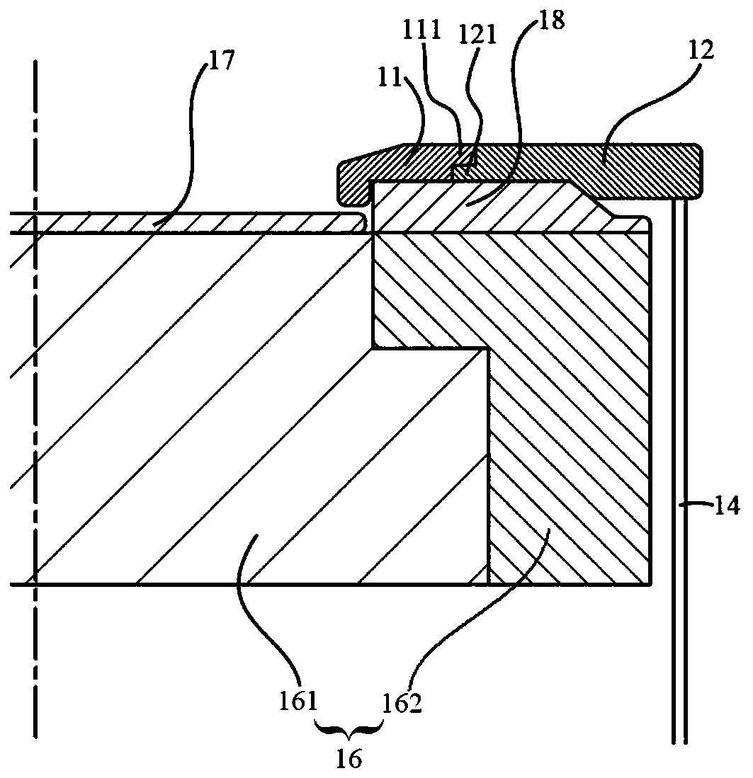
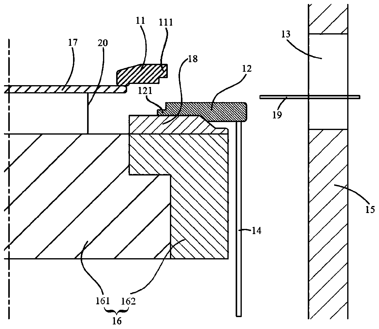
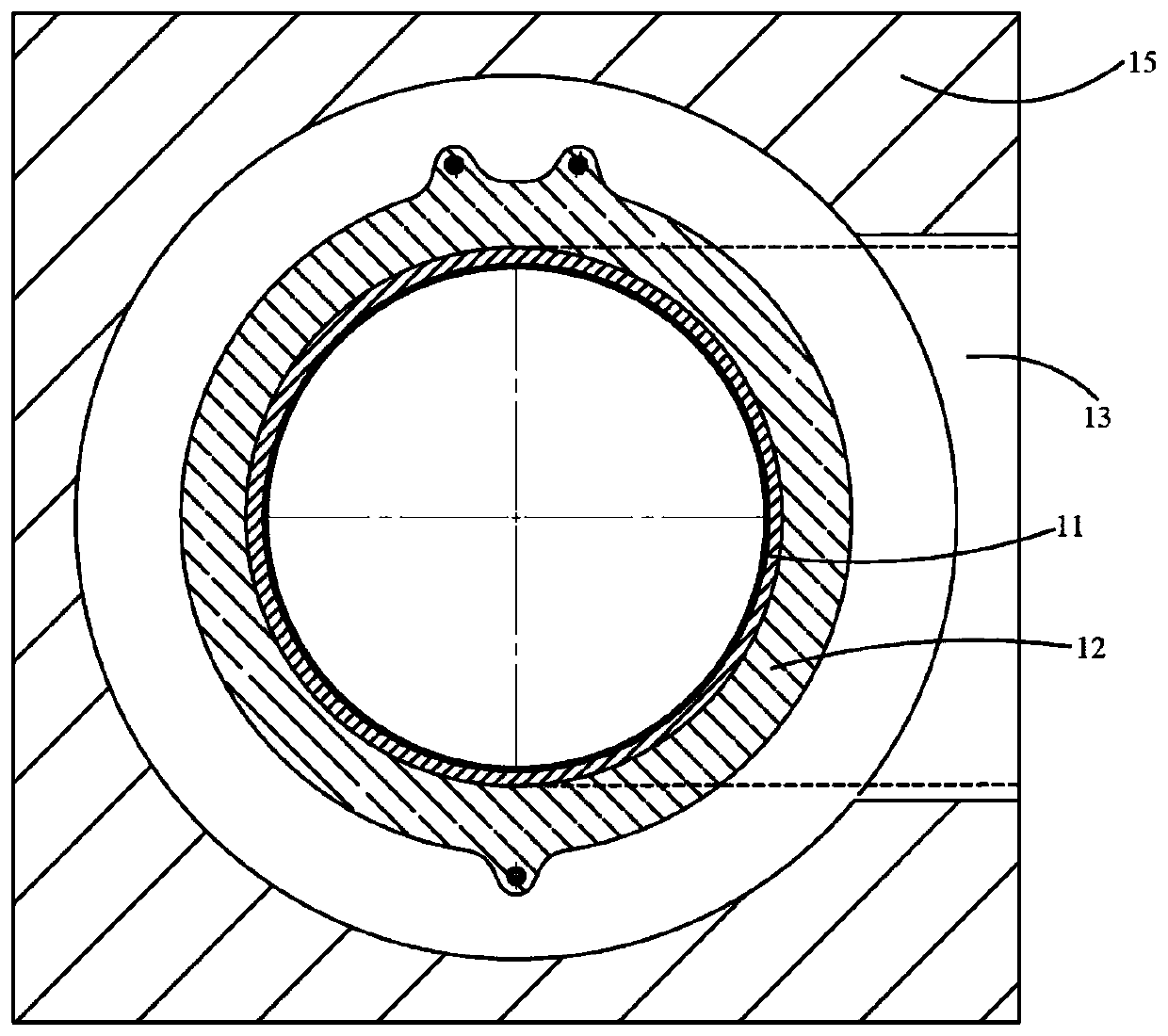
[0033] Such as Figure 1-Figure 3 As shown, the present embodiment provides a semiconductor process chamber. The semiconductor process chamber includes a base 16 and a wafer edge protection device, and the wafer edge protection device is arranged on the base 16. The wafer edge protection device includes an inner protection ring 11 and a wafer edge protection device. The outer protective ring 12; the outer protective ring 12 is arranged around the outer side of the inner protective ring 11, and is overlapped with the inner protective ring 11, and the outer protective ring 12 can drive the inner protective ring 11 to rise and fall synchronously; the inner diamete...


PUM

PropertyMeasurementUnit
thicknessaaaaaaaaaa
widthaaaaaaaaaa

Abstract

The invention provides a semiconductor process chamber, a wafer edge protection method and semiconductor equipment. The semiconductor process chamber comprises a base and a wafer edge protection device, the wafer edge protection device is arranged on the base, and the wafer edge protection device comprises an inner protection ring and an outer protection ring, the outer protection ring is arrangedon the outer side of the inner protection ring in a surrounding mode, is in lap joint with the inner protection ring and can drive the inner protection ring to ascend and descend synchronously, the inner diameter of the inner protection ring is smaller than the diameter of the wafer, the inner protection ring is used for shielding the edge of the wafer arranged on the base, and the outer diameterof the inner protection ring is smaller than the size of a wafer transfer port of the semiconductor process chamber. According to the semiconductor process chamber, the wafer edge protection method and the semiconductor equipment provided by the invention, switching of different semiconductor processing technologies can be facilitated, the productivity is improved, the uniformity of the semiconductor processing technologies can be improved, and the problem of angle inclination of the edge of the wafer in the semiconductor processing technologies is improved.

Description

technical field [0001] The invention relates to the technical field of semiconductor equipment, in particular to a semiconductor process chamber, a wafer edge protection method and semiconductor equipment. Background technique [0002] At present, since it is difficult for the mask layer to protect the curved edge of the wafer, a liftable wafer edge protection ring is usually installed in the semiconductor process chamber for the plasma etching process. The round edge protection ring is mainly used to lower the edge of the wafer to a position where it can cover the edge of the wafer in a non-contact manner during the deep groove etching process, so as to adjust the plasma density near the edge of the wafer and avoid the deep groove etching process. The medium-to-high-concentration plasma over-etches the edge of the wafer, resulting in defects such as needle-like structures and angle tilts on the edge of the wafer. However, when the shallow groove etching process is performe...

Claims


Application Information

Patent Timeline
Patent Type & Authority Applications(China)
IPC IPC(8): H01J37/02H01J37/20H01J37/305H01J37/32
CPCH01J37/3053H01J37/20H01J37/023H01J37/32385H01J37/32633H01J37/32715
Inventor 唐希文陈景春
Owner BEIJING NAURA MICROELECTRONICS EQUIP CO LTD
Why Eureka
Try Eureka