Semiconductor deposition process compensating method, compensating device and semiconductor deposition equipment

A technology of deposition process and compensation method, which is applied in the direction of metal material coating process, ion implantation plating, coating, etc., can solve the problems of inflexibility and incomplete parameter compensation method, and achieve the effect of low fitting difficulty

Active Publication Date: 2020-08-11
BEIJING NAURA MICROELECTRONICS EQUIP CO LTD
View PDF7 Cites 0 Cited by
  • Summary
  • Abstract
  • Description
  • Claims
  • Application Information

AI Technical Summary

Problems solved by technology

[0006] The purpose of the present invention is to propose a semiconductor deposition process compensation method, compensation device and deposition equipment, which can solve the problem of incomplete and inflexible existing parameter compensation methods

Method used


Image

  • Semiconductor deposition process compensating method, compensating device and semiconductor deposition equipment
  • Semiconductor deposition process compensating method, compensating device and semiconductor deposition equipment
  • Semiconductor deposition process compensating method, compensating device and semiconductor deposition equipment

Examples


Embodiment Construction

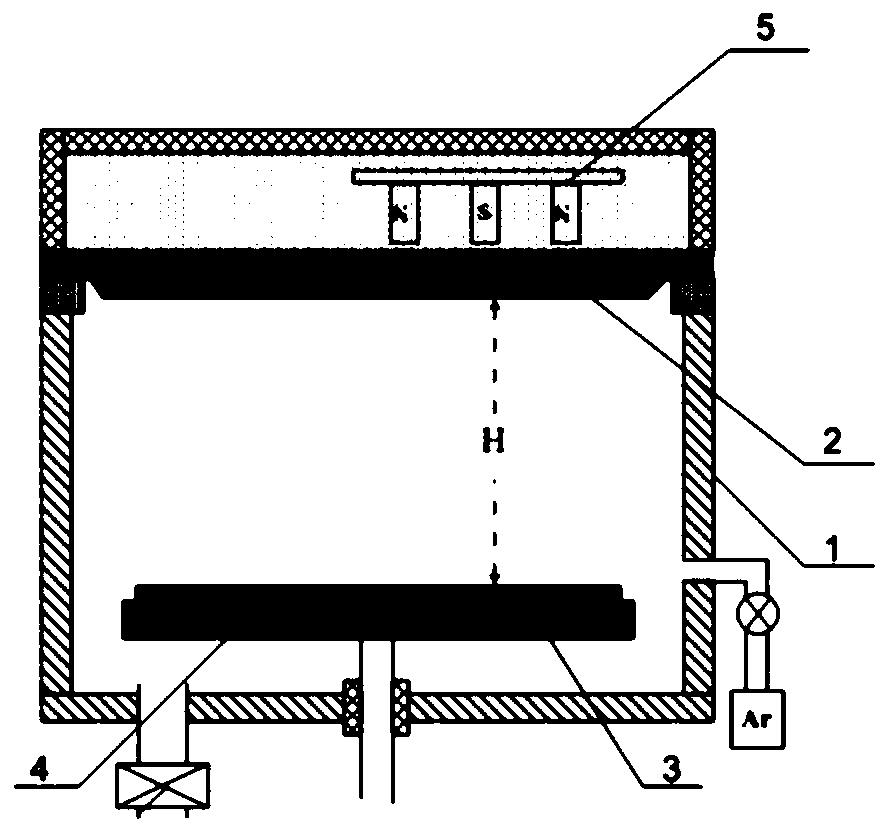
[0043] The present invention will be described in more detail below with reference to the accompanying drawings. Although preferred embodiments of the invention are shown in the drawings, it should be understood that the invention may be embodied in various forms and should not be limited to the embodiments set forth herein. Rather, these embodiments are provided so that this disclosure will be thorough and complete, and will fully convey the scope of the invention to those skilled in the art.

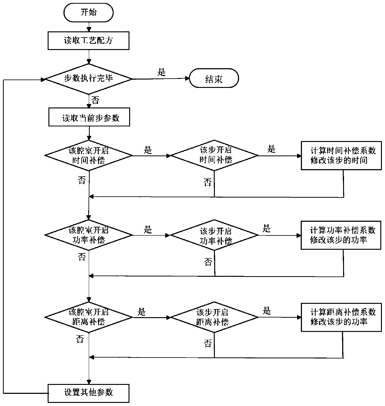
[0044] An embodiment of the present invention provides a semiconductor deposition process compensation method, figure 2 A flow chart of the steps of a semiconductor deposition process compensation method according to an embodiment of the present invention is shown. Please refer to figure 2 , the semiconductor deposition process compensation method includes the following steps:

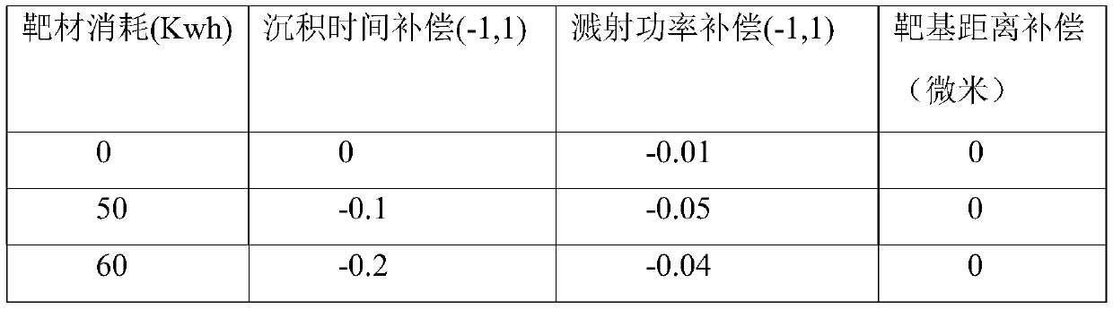
[0045] Step 1: Before executing the current process step, judge whether it is necessary to perform para...


PUM


Abstract

The invention discloses a semiconductor deposition process compensating method, a compensating device and semiconductor deposition equipment. The deposition process compensating method comprises the following steps: step 1, judging whether process parameter values of a current process step need parameter compensation or not before performing the current process step, obtaining a current target material consumption value, and calculating compensated process parameter values according to the preset multiple target material consumption values and the parameter compensation value which correspondsto each target material consumption value if the parameter compensation is needed; and step 2, performing the current process step according to the compensated process parameter values, wherein the parameter compensation values comprise at least one of the following: a deposition time compensation value, a target base distance compensation value and a sputtering power compensation value. The semiconductor deposition process compensating method has the beneficial effect that: a user can freely select independent opening time compensation, sputtering power compensation or target base distance compensation, also can simultaneously start any two or three of the ways, and flexible configuration in the step of each process formula is achieved.

Description

technical field [0001] The invention relates to the technical field of semiconductor technology, in particular to a semiconductor deposition process compensation method, a compensation device and semiconductor deposition equipment. Background technique [0002] With the rapid development of the semiconductor manufacturing industry, more and more semiconductor equipment is produced and used, such as: magnetron PVD (Physical Vapor Deposition, physical vapor deposition) equipment, etc., these semiconductor equipment need Use the target material of the corresponding material. like figure 1 The structure diagram of a typical magnetron PVD equipment is shown, including the equipment chamber 1, the target material 2 used in sputtering deposition, and the magnetron 5. The sputtering power supply outputs power to the target material 2, and the substrate holder 3 is used for The substrate 4 is contained, and the substrate seat 3 can be driven by a motor or an air cylinder to move up...

Claims


Application Information

Patent Timeline
Patent Type & Authority Applications(China)
IPC IPC(8): C23C14/54C23C14/35
CPCC23C14/54C23C14/35C23C14/3407
Inventor 曹光英
Owner BEIJING NAURA MICROELECTRONICS EQUIP CO LTD
Why Eureka
Try Eureka