Super-large-scale integrated circuit layout method considering atomization and proximity effects

A large-scale integrated circuit and proximity effect technology, which is applied in electrical digital data processing, special data processing applications, instruments, etc., can solve problems such as long running time and no consideration of proximity effect

Active Publication Date: 2020-08-14
福州立芯科技有限公司
View PDF4 Cites 0 Cited by
  • Summary
  • Abstract
  • Description
  • Claims
  • Application Information

AI Technical Summary

Problems solved by technology

However, this work did not consider the critical proximity effect
Another problem is that it takes 2.44 times longer to run compared to the layout method that does not account for fogging effects

Method used


Image

  • Super-large-scale integrated circuit layout method considering atomization and proximity effects
  • Super-large-scale integrated circuit layout method considering atomization and proximity effects
  • Super-large-scale integrated circuit layout method considering atomization and proximity effects

Examples


Embodiment Construction

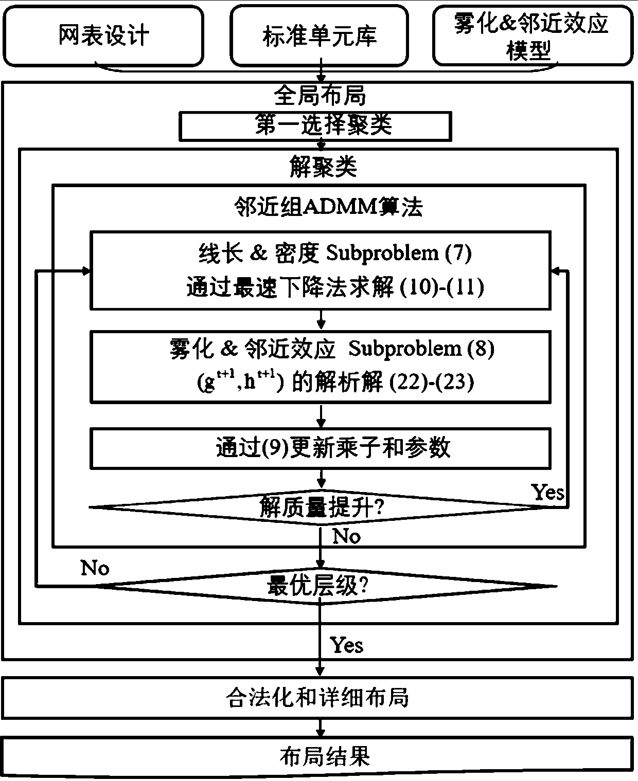
[0090] The present invention will be further described below in conjunction with the accompanying drawings and specific embodiments.

[0091] The present invention provides a VLSI layout method considering atomization and proximity effect to solve the VLSI layout problem considering atomization and proximity effect, thereby reducing the adverse effects caused by atomization and proximity effect, thereby improving layout efficiency . The basic idea of ​​this method is to formulate the global layout problem as a separable linear constraint minimization problem. According to the energy model of atomization and proximity effect, solving the targets one by one in an alternating manner, writing out the proximity group and solving it also greatly reduces the complexity of the optimization problem and reduces the computational cost, thus effectively reducing the The effects of fogging and proximity effects are eliminated. In each iteration of the method, two subproblems are solved w...


PUM


Abstract

The invention relates to a super-large-scale integrated circuit layout method considering atomization and proximity effects. The method comprises the following steps: (1) establishing an energy distribution model for the atomization and proximity effects in electron beam lithography (EBL) and describing changes of the energy distribution model; (2) optimizing a model and a function in the global layout, and determining a smooth target function; (3) introducing a new variable to convert an unconstrained minimization problem into a separable minimization problem CSMP with linear constraints; (4)determining an adjacent group ADMM algorithm and an iterative formula of the separable minimization problem; (5) solving two sub-problems in adjacent group iteration; and (6) performing convergence analysis on the ADMM algorithm of the adjacent group. The method is beneficial to reducing adverse effects caused by atomization and proximity effect and improving the layout efficiency.

Description

technical field [0001] The invention belongs to the technical field of VLSI design, and in particular relates to a VLSI layout method considering atomization and proximity effects. Background technique [0002] Since EBL can print fine patterns, it is used for patterning at sub-22nm process nodes and above. The electron gun directly emits electrons through a set of lenses and apertures to carve patterns on the wafer. When the primary electron beam from the electron gun hits the resistor and the substrate, the electrons may scatter. The scattered electrons produce backscattered electrons, which may hit the bottom of the objective. As a result, the impact may generate a next generation of electrons, so-called rescattered electrons. These scattered, backscattered, and rescattered electrons can cause unwanted exposure, resulting in proximity and fogging effects. [0003] Proximity effects are produced by scattered and backscattered electrons. More precisely, scattered elect...

Claims


Application Information

Patent Timeline
IPC IPC(8): G06F30/3308G06F30/392
CPCG06F30/3308G06F30/392
Inventor 陈建利林智峰黄志鹏
Owner 福州立芯科技有限公司
Why Eureka
Try Eureka