Substrate cleaning method, substrate cleaning apparatus and storage medium
A technology for cleaning devices and storage media, applied in cleaning methods and utensils, cleaning methods using tools, chemical instruments and methods, etc., capable of solving problems such as insufficient cleaning
- Summary
- Abstract
- Description
- Claims
- Application Information
AI Technical Summary
Problems solved by technology
Method used
Image

Examples
Embodiment Construction
[0034] Hereinafter, embodiments of the present disclosure will be specifically described with reference to the drawings.
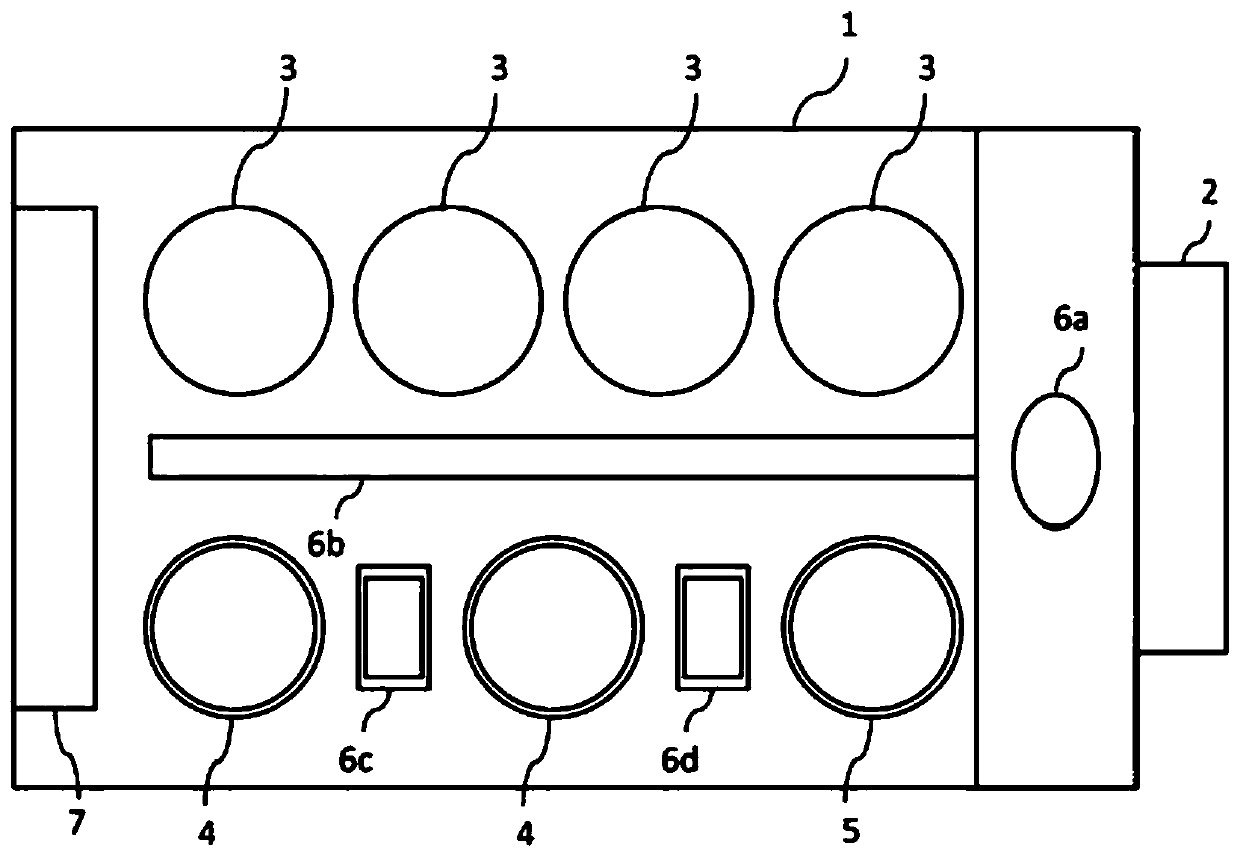
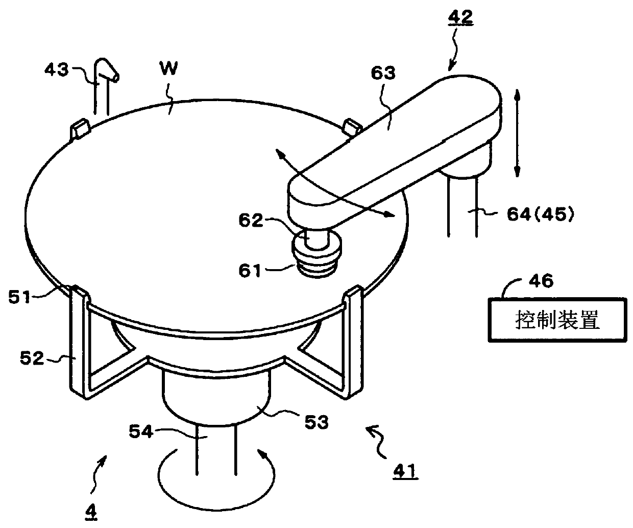
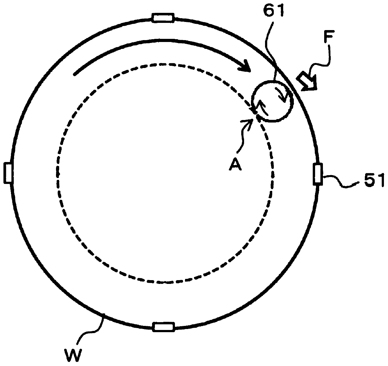
[0035] figure 1It is a schematic plan view of the substrate processing apparatus of one embodiment. This substrate processing device is a semiconductor wafer with a diameter of 300 mm or 450 mm, a flat panel, an image sensor such as CMOS (Complementary Metal Oxide Semiconductor) or CCD (Charge Coupled Device: Charge Coupled Device), and MRAM (Magnetoresistive Random Access Memory: A device for processing various substrates in the manufacturing process of the magnetic film in magnetoresistive random access memory). In addition, the shape of the substrate is not limited to a circle, and may be a rectangular shape (square shape) or a polygonal shape.
[0036] The substrate processing apparatus includes: a substantially rectangular housing 1, a loading port 2 for loading and storing a plurality of substrate cassettes, and one or more (in figure 1 In the sho...
PUM
 Abstract
Description
Claims
Application Information
 - R&D Engineer
- R&D Manager
- IP Professional
- Industry Leading Data Capabilities
- Powerful AI technology
- Patent DNA Extraction
Browse by: Latest US Patents, China's latest patents, Technical Efficacy Thesaurus, Application Domain, Technology Topic.
© 2024 PatSnap. All rights reserved.Legal|Privacy policy|Modern Slavery Act Transparency Statement|Sitemap