CNN (Convolutional Neural Network) visualization-based PCB (Printed Circuit Board) defect detection method

A technology for PCB circuit board and defect detection, applied in image data processing, image enhancement, instruments, etc., can solve problems such as poor interpretability, and the working principle of deep neural network cannot be described in words, so as to improve generalization. Effect

Pending Publication Date: 2020-08-25
FOSHAN NANHAI GUANGDONG TECH UNIV CNC EQUIP COOP INNOVATION INST +1
View PDF3 Cites 7 Cited by
  • Summary
  • Abstract
  • Description
  • Claims
  • Application Information

AI Technical Summary

Problems solved by technology

[0002] For a long time, CNN has been controversial despite its remarkable effect. The root cause is its poor interpretability. How did the neural network produce this result? Especially when the number of layers of the neural network is large, the interpretability is very poor, and the working principle of the deep neural network cannot be described in words. Therefore, before the emergence of convolution visualization, it has been regarded as a "black box".

Method used


Image

  • CNN (Convolutional Neural Network) visualization-based PCB (Printed Circuit Board) defect detection method
  • CNN (Convolutional Neural Network) visualization-based PCB (Printed Circuit Board) defect detection method
  • CNN (Convolutional Neural Network) visualization-based PCB (Printed Circuit Board) defect detection method

Examples


Embodiment 1

[0030] Such as Figure 1 to Figure 4 As shown, the present embodiment discloses a method for detecting defects of a PCB circuit board based on CNN visualization, and the detection method mainly includes the following specific steps:

[0031] Step S1: Collect PCB circuit board defect images and normal images, and then make training and verification data sets {(TrainX1, TrainY1), (TestX1, TestY1)} to be used for training;

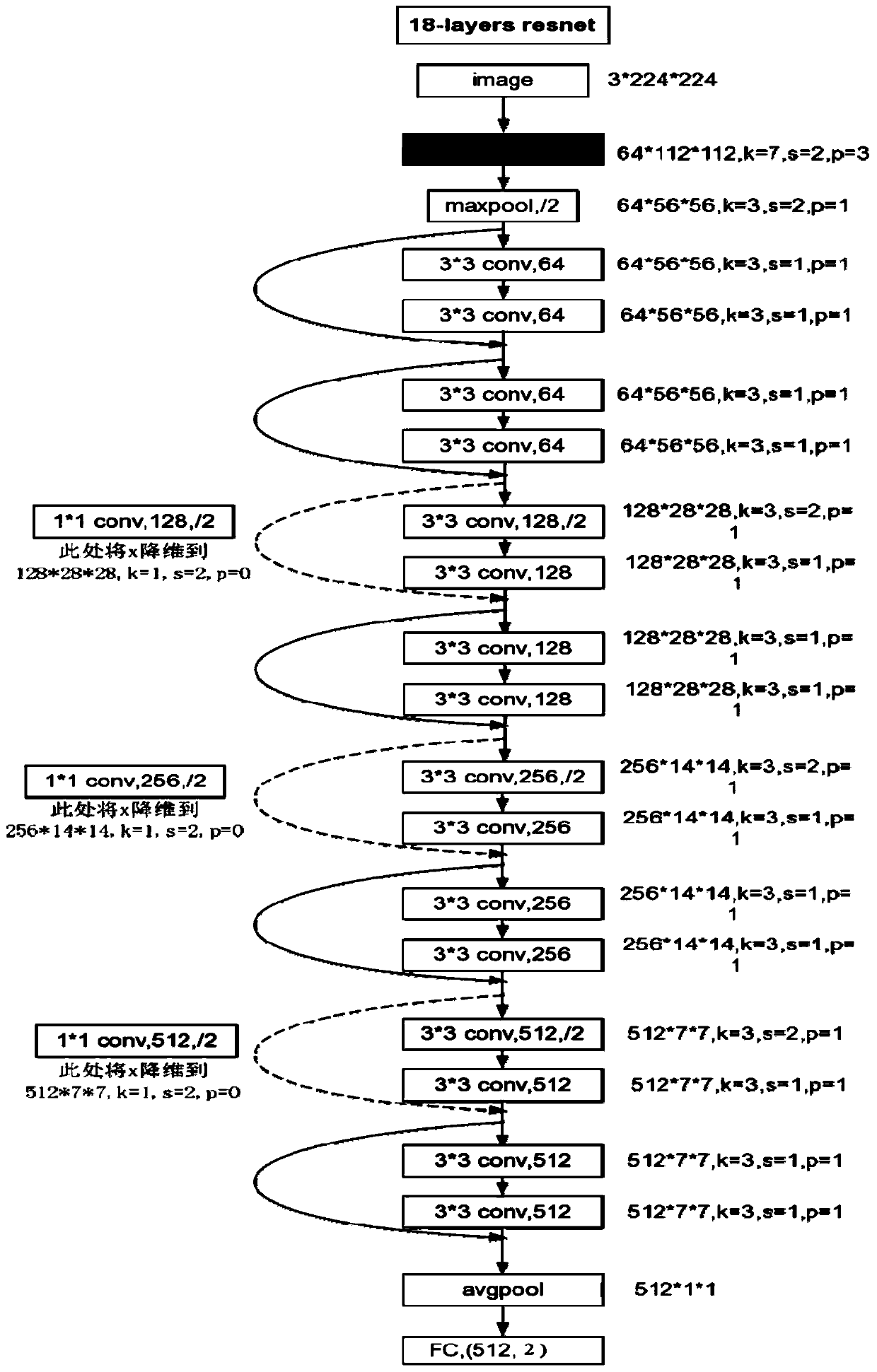
[0032] Step S2: Build a PCB circuit board defect detection and recognition model, and use the data set produced in step S1 to study circuit board defects, and obtain a preliminary recognition model Model1;

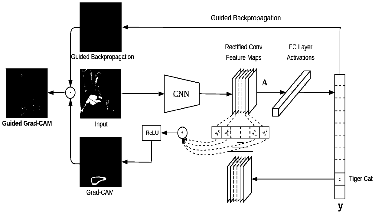
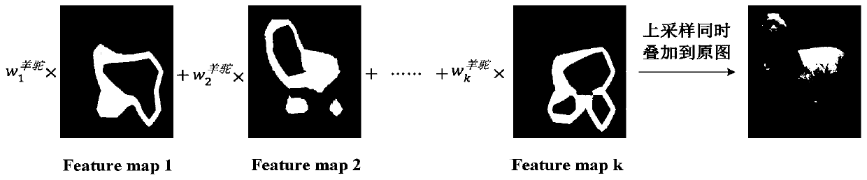
[0033] Step S3: Calculate and design the CNN visualization model (MapModel), by calculating the neuron importance weight w k , and then calculate the weighted sum of the corresponding feature map, and superimpose it on the original image after upsampling to obtain the category positioning heat map;

[0034] Step S4: Check the category positioning heat m...

Embodiment 2

[0044] This embodiment discloses a PCB circuit board defect detection method based on CNN visualization, comprising the following steps:

[0045]Step S1, collecting PCB circuit board defect images and normal images, and then making training and verification data sets {(TrainX1, TrainY1), (TestX1, TestY1)} to be used for training.

[0046] Step S2, build a PCB circuit board defect detection and recognition model, and use the data set produced in step S1 to study circuit board defects, and obtain a preliminary recognition model Model1.

[0047] Step S3, calculate and design the CNN visualization model (MapModel), calculate the weighted sum of the corresponding feature maps by calculating the neuron importance weight wk, and then superimpose on the original image after upsampling to obtain the category positioning heat map.

[0048] Step S4, check the category positioning heat map generated by the original image data through the CNN visualization model (MapModel), and check wheth...

Embodiment 3

[0064] This embodiment discloses a method for detecting defects of a PCB circuit board based on CNN visualization, which is characterized in that it includes the following implementation steps:

[0065] Step S1, collecting PCB circuit board defect images and normal images, and then making training and verification data sets {(TrainX1, TrainY1), (TestX1, TestY1)} to be used for training.

[0066] Step S1-1, use an industrial camera to capture the entire picture of the PCB circuit board on the actual production line, and then divide it into small pictures of 224×224 pixels to facilitate the identification of small defects and model training.

[0067] Step S1-2, manually mark and classify the divided 224×224 pictures, divide them into defective and non-defective categories, and ensure the balance of the data. The data volume of the two categories is 1:1, and then the data According to 9:1, it is divided into two parts, the more data is used as the training set (TrainX1, TrainY1),...


PUM


Abstract

The invention discloses a CNN (Convolutional Neural Network) visualization-based PCB (Printed Circuit Board) defect detection method, which overcomes the problem of poor interpretability of a convolutional neural network, corrects training data errors by utilizing a CNN model and combining model visualization of the CNN model, and checks the accuracy of model category positioning to improve the precision of defect detection. The method comprises the following steps: training acquired PCB image data through a convolutional neural network; then positioning a thermodynamic diagram through Grad-CAM categories to judge whether the basis for predicting the visualization model is correct or not, detecting the cause of a data error of a prediction error, and then adjusting the data to reduce the error of a training set, thereby achieving the purpose of improving the precision of the data set.

Description

technical field [0001] The invention relates to the technical field of deep learning computer vision, in particular to a method for detecting defects of PCB circuit boards based on CNN visualization. Background technique [0002] For a long time, CNN has been controversial despite its remarkable effect. The root cause is its poor interpretability. How did the neural network produce this result? Especially when the number of layers of the neural network is large, the interpretability is very poor, and the working principle of the deep neural network cannot be described in words. Therefore, before the emergence of convolution visualization, it has been regarded as a "black box". But the reality is that our users or terminals need interpretability, so the research field of convolution visualization has been derived. [0003] The Grad-CAM (Gradient-weighted Class Activation Mapping) method can make the CNN model interpretable and transparent. By calculating the neuron importanc...

Claims


Application Information

Patent Timeline
Patent Type & Authority Applications(China)
IPC IPC(8): G06T7/00G06K9/34G06K9/62G06N3/04
CPCG06T7/0004G06T2207/30141G06V10/267G06N3/045G06F18/214
Inventor 杨海东李俊宇黄坤山彭文瑜林玉山魏登明
Owner FOSHAN NANHAI GUANGDONG TECH UNIV CNC EQUIP COOP INNOVATION INST
Why Eureka
Try Eureka