A kind of multi-layer organic substrate and manufacturing method

A technology of organic substrates and manufacturing methods, which is applied in the fields of multilayer circuit manufacturing, removal of conductive materials by chemical/electrolytic methods, and printed circuit manufacturing. Suitable for problems such as extremely high layers and high thickness requirements of MLO substrates, high cost, etc., to achieve the effect of improving product competitiveness, excellent electrical performance, and lowering the manufacturing threshold

Active Publication Date: 2021-06-25
SHANGHAI ZENFOCUS SEMI-TECH CO LTD
View PDF0 Cites 0 Cited by
  • Summary
  • Abstract
  • Description
  • Claims
  • Application Information

AI Technical Summary

Problems solved by technology

Due to the extremely high line density requirements for MLO docking and chip layer C4, the subtractive process used in traditional PCB / BGA can no longer be produced, and even the mSAP process commonly used in Substrate is difficult to meet the requirements. The latest technical requirements can only be used in Japan. Universiade Ajinomoto’s ABF film’s full-additive SAP process, this electroplating process is mostly used for packaging substrates in high-performance computing fields such as high-end CPU / GPU due to its high cost, technically limit line width / line spacing ( 15 / 15um), the production of MLO based on the existing process requires more than 10 lines, pressing and drilling processes, the process is complex, the cost is high, the delivery period is long, and the technology has reached a bottleneck, and it is difficult to continue to advance
[0004] Embedded circuit technology originates from the ancient damascene process (damascene process), which is used in high-density additive / semi-additive wiring in the field of semiconductor packaging. It is suitable for making a single high-density wiring layer of packaging substrates. It is generally used In the field of thin substrates with a small number of layers, the number of increments generally does not exceed 3 times. The more layers, the higher the cost compared with the traditional double-sided layer buildup process. The embedded circuit process still accounts for a relatively low proportion in the current packaging substrate field. , the single buried line process cannot be suitable for MLO substrates with extremely high layer count and high thickness requirements

Method used


Image

  • A kind of multi-layer organic substrate and manufacturing method
  • A kind of multi-layer organic substrate and manufacturing method
  • A kind of multi-layer organic substrate and manufacturing method

Examples


Embodiment Construction

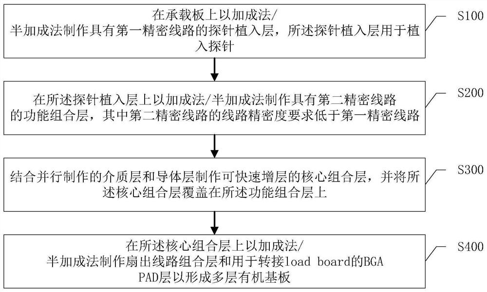
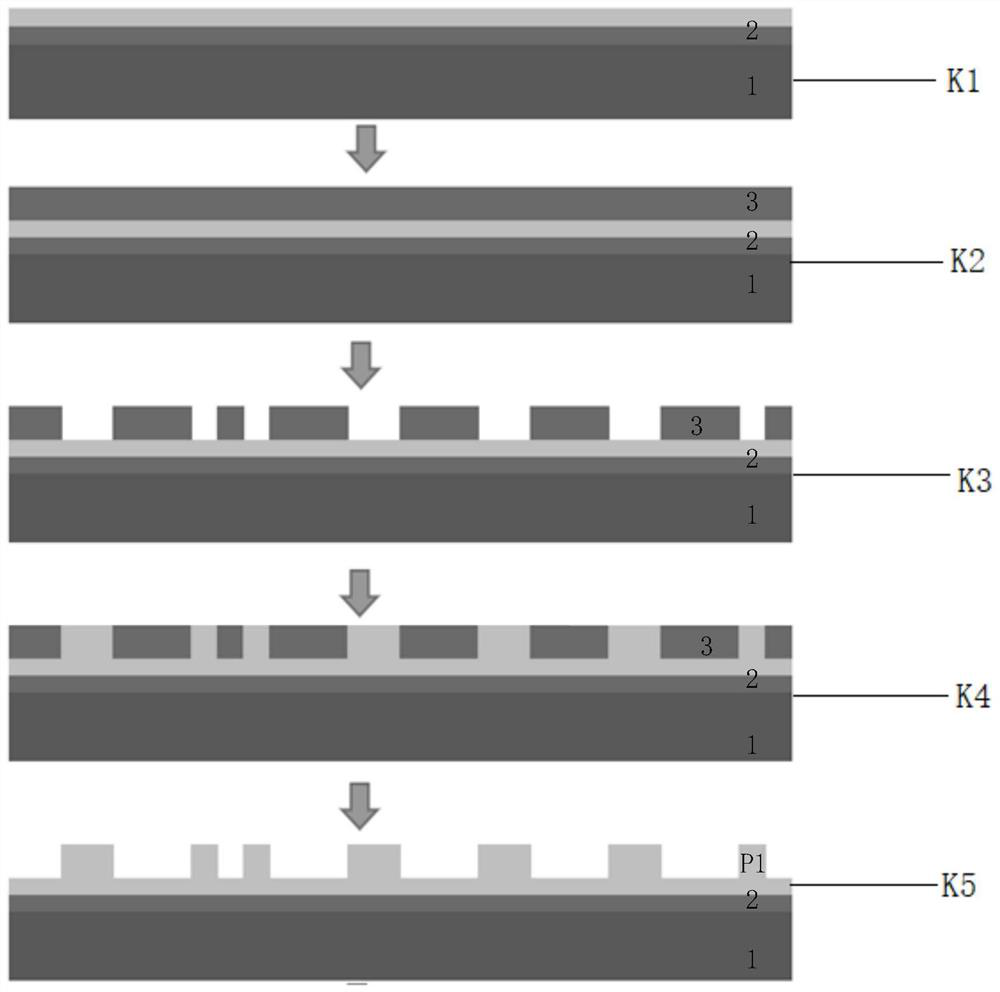
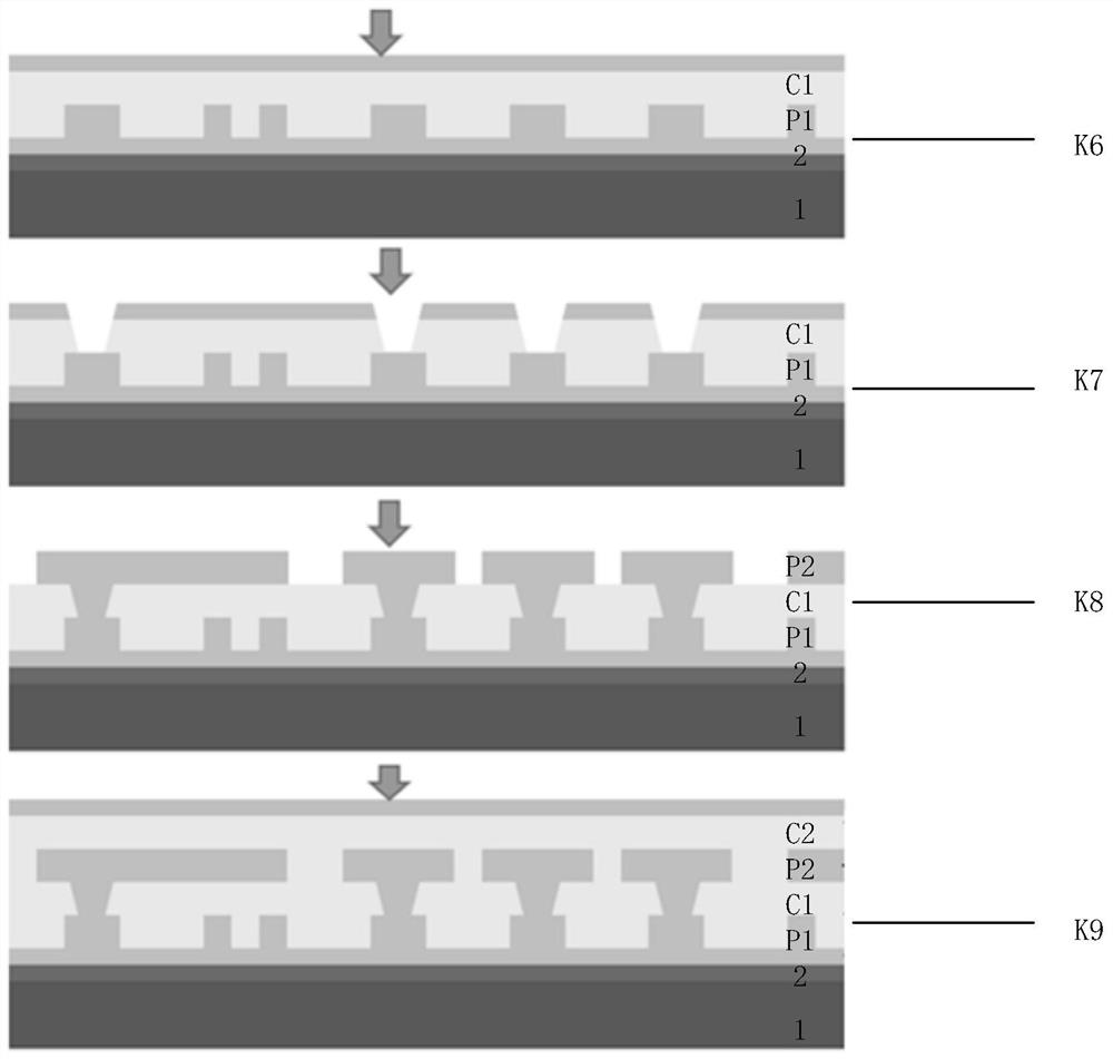
[0060] In order to more clearly illustrate the embodiments of the present invention or the technical solutions in the prior art, the specific implementation manners of the present invention will be described below with reference to the accompanying drawings. Obviously, the accompanying drawings in the following description are only some embodiments of the present invention, and those skilled in the art can obtain other accompanying drawings based on these drawings and obtain other implementations.

[0061] In order to make the drawing concise, each drawing only schematically shows the parts related to the present invention, and they do not represent the actual structure of the product. In addition, to make the drawings concise and easy to understand, in some drawings, only one of the components having the same structure or function is schematically shown, or only one of them is marked. Herein, "a" not only means "only one", but also means "more than one".

[0062] An embodim...


PUM


Abstract

The technical field of the present invention is the field of semiconductor testing, providing a multi-layer organic substrate and a manufacturing method, the method comprising: manufacturing a probe implant with a first precision circuit on the carrier board by an additive method / semi-additive method layer; on the probe implantation layer, a functional combination layer with a second precision circuit is produced by an additive method / semi-additive method, wherein the circuit precision requirement of the second precision circuit is lower than that of the first precision circuit; combined with the parallel production The dielectric layer and the conductor layer are used to make a core composite layer that can be rapidly increased, and the core composite layer is covered on the functional composite layer; on the core composite layer, the fan-out circuit composite layer is made by additive method / semi-additive method and used for Transfer the BGA PAD layer of the load board to form a multi-layer organic substrate. The present invention realizes a low-cost, short-production-cycle multilayer organic substrate manufacturing method, thereby reducing the minimum C4 Pad spacing of the multilayer organic substrate and improving the wiring density of the probe implantation layer, while the C4 Pad surface can be ultra-flat Spend.

Description

technical field [0001] The invention relates to the field of semiconductor testing, in particular to a multilayer organic substrate and a manufacturing method. Background technique [0002] MLO is the abbreviation of Multi layered Organic substrate, which is multi-layered organic substrate in Chinese, which is used to carry vertical probe cards to test uncut wafers; the size of the probes implanted on MLO needs to match the size of the wafer under test. The contact (C4 Pad), so this requires the MLO substrate to have a high-precision circuit layer (C4 Side), needle planting and testing require the substrate to have high rigidity and strength, usually by increasing the total board thickness to meet the requirements, wafer testing Probes are required to have good coplanarity, which requires that the MLO substrate on which the probes are implanted has good surface flatness. [0003] The existing manufacturing method of the MLO multilayer organic substrate is the traditional co...

Claims


Application Information

Patent Timeline
Patent Type & Authority Patents(China)
IPC IPC(8): H05K3/46H05K3/06H05K3/00H05K3/42H05K3/28H05K1/02H05K1/11
CPCH05K1/0298H05K1/115H05K3/0026H05K3/0047H05K3/0094H05K3/06H05K3/282H05K3/423H05K3/4644
Inventor 陶克文罗雄科袁凯华
Owner SHANGHAI ZENFOCUS SEMI-TECH CO LTD
Why Eureka
Try Eureka