Supercharge Your Innovation With Domain-Expert AI Agents!

Thick film optical waveguide and method of making the same

A manufacturing method and optical waveguide technology, applied in the direction of optical waveguide light guide, light guide, optics, etc., can solve problems such as thick film light wave cracks, achieve the effect of overcoming cracks and warping, and avoiding stress accumulation

Active Publication Date: 2022-08-05
UNITED MICROELECTRONICS CENT CO LTD
View PDF5 Cites 0 Cited by
  • Summary
  • Abstract
  • Description
  • Claims
  • Application Information

AI Technical Summary

Problems solved by technology

[0004] The invention provides a thick-film optical waveguide and a manufacturing method thereof, which are used to solve the problem that the thick-film optical waveguide is prone to cracks in the prior art, so as to improve the performance of the thick-film optical waveguide

Method used


Image

  • Thick film optical waveguide and method of making the same
  • Thick film optical waveguide and method of making the same
  • Thick film optical waveguide and method of making the same

Examples


Embodiment Construction

[0051] The specific embodiments of the thick film optical waveguide and the manufacturing method thereof provided by the present invention will be described in detail below with reference to the accompanying drawings.

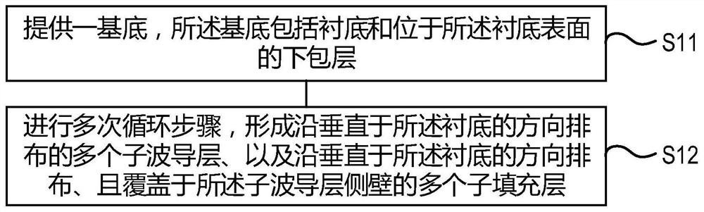
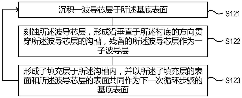
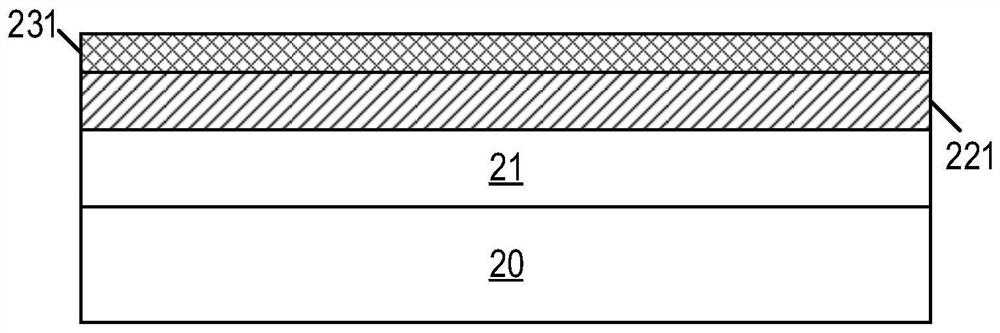
[0052] This specific embodiment provides a thick film optical waveguide with attached Figure 1A It is the flow chart of the method for forming the thick film optical waveguide in the specific embodiment of the present invention, with the attached Figure 1B is the flow chart of the cycle steps in the specific embodiment of the present invention, with the attached Figures 2A-2J It is a schematic cross-sectional schematic diagram of the main process in the process of forming the thick-film optical waveguide in the specific embodiment of the present invention. like Figure 1A , Figure 1B , Figures 2A-2J As shown, the method for manufacturing a thick-film optical waveguide provided by this specific embodiment includes the following steps:

[0053] In step S1...


PUM

PropertyMeasurementUnit
thicknessaaaaaaaaaa
thicknessaaaaaaaaaa
thicknessaaaaaaaaaa

Abstract

The present invention relates to a method for manufacturing a thick film waveguide. The manufacturing method of the thick-film optical waveguide includes the steps of: providing a substrate; performing multiple cycle steps to form a plurality of sub-waveguide layers arranged in a direction perpendicular to the substrate, and forming a plurality of sub-waveguide layers along a direction perpendicular to the substrate. a plurality of sub-filling layers arranged in a direction and covering the sidewalls of the sub-waveguide layers; the cycle step includes: depositing a waveguide core layer on the surface of the substrate; etching the waveguide core layer to form a through-waveguide layer In the trench of the core layer, the remaining waveguide core layer is used as a sub-waveguide layer; a sub-filling layer is formed in the trench, and the surface of the sub-filling layer and the surface of the sub-waveguide layer are jointly used as the bottom layer. Substrate surface for one cycle step. The invention overcomes the problems of cracking and warping caused by depositing a thick waveguide core layer at one time, reduces the transmission loss of the waveguide, and effectively improves the performance of the thick-film optical waveguide.

Description

technical field [0001] The present invention relates to the technical field of semiconductor manufacturing, and in particular, to a method for manufacturing a thick-film waveguide. Background technique [0002] An optical waveguide is a medium device that guides light waves to propagate in it, and is also called a medium optical waveguide. In the existing production process, there are mainly two ways to form thick-film optical waveguides: one is to deposit the waveguide material for many times and then dry etching to form it; the other is to form trenches in the lower cladding layer first, The trenches are then filled with waveguide material to form. However, the area without cracks in the thick-film optical waveguide obtained by the method of depositing the waveguide material for many times is small; in the method of trench filling, due to factors such as insufficiently steep sidewalls and insufficiently flat bottoms of the trenches, the resulting thick The roughness of t...

Claims


Application Information

Patent Timeline
Patent Type & Authority Patents(China)
IPC IPC(8): G02B6/136G02B6/13G02B6/122
CPCG02B6/136G02B6/13G02B6/122G02B2006/12176G02B2006/12166
Inventor 何来胜朱继光王琬箐
Owner UNITED MICROELECTRONICS CENT CO LTD
Features
  • R&D
  • Intellectual Property
  • Life Sciences
  • Materials
  • Tech Scout
  • Unparalleled Data Quality
  • Higher Quality Content
  • 60% Fewer Hallucinations
Learn More