Supercharge Your Innovation With Domain-Expert AI Agents!

Red light semiconductor laser of aluminum-free active region and preparation method of red light semiconductor laser

An active region and semiconductor technology, applied in the field of optoelectronics, can solve the problems of high material growth requirements, easy formation of defects, affecting laser performance, etc., to reduce light absorption, reduce the formation of cavity surface defects, and improve the effect of burning resistance.

Active Publication Date: 2022-05-27
Shandong Huaguang Optoelectronics Co. Ltd.
View PDF15 Cites 0 Cited by
  • Summary
  • Abstract
  • Description
  • Claims
  • Application Information

AI Technical Summary

Problems solved by technology

[0005] In order to solve the disadvantages that the waveguide layer of the existing red semiconductor laser is made of aluminum-containing material, which requires high material growth, and is easy to form defects, which affects the performance of the laser, the invention provides a red semiconductor laser without an aluminum active region As well as the preparation method, adjust the composition of the GaInAsP quaternary alloy to achieve lattice matching with the GaAs substrate and avoid stress accumulation during the growth process; optimize the growth conditions to reduce the impact of the large surface roughness of the quaternary alloy on the material properties; use GaInAsP As a waveguide layer, GaInP as a quantum well, to achieve aluminum-free active region design

Method used


Image

  • Red light semiconductor laser of aluminum-free active region and preparation method of red light semiconductor laser
  • Red light semiconductor laser of aluminum-free active region and preparation method of red light semiconductor laser
  • Red light semiconductor laser of aluminum-free active region and preparation method of red light semiconductor laser

Examples


Embodiment 1

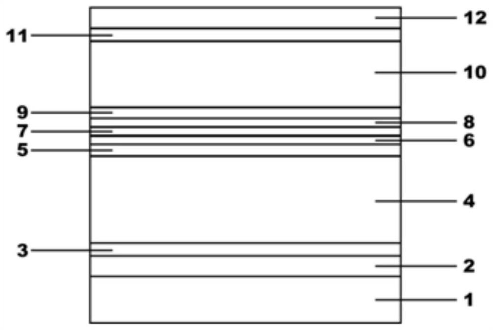
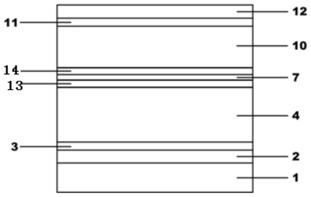
[0093] A red light semiconductor laser with no aluminum active region, such as figure 1 As shown, it includes GaAs substrate 1 , GaAs buffer layer 2 , GaAs x1 In 1-x1 P lower transition layer 3, AlGaInP lower confinement layer 4, Ga x5 In 1-x5 As y4 P 1-y4 Lower waveguide layer 5, Ga 1-x6 In x6 P lower barrier layer 6, Ga 1-x7 In x7 P quantum well 7, Ga 1-x8 In x8 P upper barrier layer 8, Ga x9 In 1-x9 As y5 P 1-y5 Upper waveguide layer 9, AlGaInP upper confinement layer 10, Ga 1-x12 In x12 P upper transition layer 11 and GaAs cap layer 12;

[0094] The AlGaInP lower confinement layer 4 includes (Al 1-x2 Ga x2 ) y1 In 1-y1 P lower confinement layer-1, (Al 1- x3 Ga x3 ) y2 In 1-y2 P lower confinement layer-2, (Al 1-x4 Ga x4 ) y3 In 1-y3 P lower limit layer -3;

[0095] The AlGaInP upper confinement layer 10 includes (Al 1-x10 Ga x10 ) y6 In 1-y6 P upper confinement layer-1, (Al 1-x11 Ga x11 ) y7 In 1-y7 P upper limit layer-2;

[0096] Amon...

Embodiment 2

[0105] A red light semiconductor laser without aluminum active region according to Embodiment 1, the difference is: Ga x5 In 1- x5 As y4 P 1-y4 The thickness of the lower waveguide layer 5 is 0.1-0.3 μm, unintentionally doped; Ga x9 In 1-x9 As y5 P 1-y5 The thickness of the upper waveguide layer 9 is 0.1-0.3 μm, unintentionally doped; Ga 1-x7 In x7 The P quantum well 7 has a thickness of 5-10 nm and is unintentionally doped.

Embodiment 3

[0107] A red light semiconductor laser without an aluminum active region according to Embodiment 1, the difference is: x5=0.9, y4=0.8. Ga x5 In 1-x5 As y4 P 1-y4 The thickness of the lower waveguide layer 5 is 0.2 μm. x9=0.9, y5=0.8. Ga x9 In 1-x9 As y5 P 1-y5 The thickness of the upper waveguide layer 9 is 0.13 μm. x7=0.65. Ga x5 In 1-x5 As y4 P 1-y4 Lower waveguide layer 5, Ga x9 In 1-x9 As y5 P 1-y5 The value of the composition of the upper waveguide layer 9 is to adjust the band gap and lattice constant, while the Ga x5 In 1-x5 As y4 P 1-y4 Lower waveguide layer 5, Ga x9 In 1- x9 As y5 P 1-y5 The thickness of the upper waveguide layer 9 is different, the purpose is to control the shift of the light field in the light emitting area to the N side, and reduce the loss caused by the carrier to the light absorption.

[0108] Ga 1-x7 In x7 The thickness of the P quantum well 7 is 7 nm. Ga 1-x7 In x7 The P quantum well 7 has different components, d...


PUM

PropertyMeasurementUnit
thicknessaaaaaaaaaa
thicknessaaaaaaaaaa
thicknessaaaaaaaaaa

Abstract

The invention relates to a red light semiconductor laser without an aluminum active region and a preparation method thereof. The red light semiconductor laser comprises a GaAs substrate, a GaAs buffer layer, a Gax1In (1-x) 1P transition layer, an AlGaInP lower limiting layer, a Gax5In (1-x) 5Asy4P (1-y) 4 lower waveguide layer, a Ga (1-x) 6Inx6P lower barrier layer, a Ga (1-x) 7Inx7P quantum well, a Ga (1-x) 8Inx8P upper barrier layer, a Gax9In (1-x) 9Asy5P (1-y) 5 upper waveguide layer, an AlGaInP upper limiting layer, a Ga (1-x) 12Inx12P upper transition layer and a GaAs cap layer which are sequentially arranged from bottom to top. According to the invention, the aluminum-free active region design is realized, the oxidation resistance is increased during cavity surface dissociation, the formation of cavity surface defects is reduced, the light absorption is reduced, the anti-burning capacity of the cavity surface is improved, and the service life of the semiconductor laser is prolonged.

Description

technical field [0001] The invention relates to the technical field of optoelectronics, in particular to a red light semiconductor laser device without an aluminum active area and a preparation method thereof. Background technique [0002] The red semiconductor laser has the advantages of small size, long life and high photoelectric conversion efficiency. It gradually replaces the traditional He-Ne gas laser and ruby ​​solid-state laser, and is widely used in optical storage systems, barcode readers, industrial alignment and marking instruments, medical Health care equipment and other fields. Among them, the wavelength selection of the red light source of laser display devices such as laser TVs and portable projectors mainly considers two factors: 1) According to the responsivity of the human eye to the wavelength, the wavelength that the human eye is sensitive to is selected to obtain higher light 2) The selected wavelength can expand the coverage of the color gamut, so as...

Claims


Application Information

Patent Timeline
Patent Type & Authority Applications(China)
IPC IPC(8): H01S5/20H01S5/34H01S5/343
CPCH01S5/3407H01S5/34373H01S5/2013Y02P70/50
Inventor 刘飞朱振于军辛欣
Owner Shandong Huaguang Optoelectronics Co. Ltd.
Features
  • R&D
  • Intellectual Property
  • Life Sciences
  • Materials
  • Tech Scout
  • Unparalleled Data Quality
  • Higher Quality Content
  • 60% Fewer Hallucinations
Learn More